A Specialized 1.2V to 3.3V Fail-Safe GPIO in Dongbu HiTek 110nm 11SB Pro- cess, with multiple protocol capabilties.
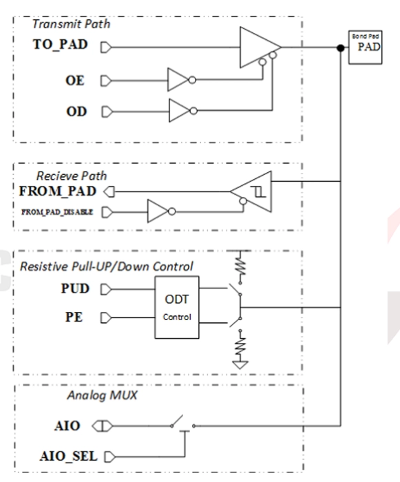
This silicon-proven Wirebond compatible library in Dongbu HiTek 110nm features a multi-voltage, multi-standard General Purpose Input Output with an Open-Drain Input Output capability, that targets the I2C standard. The library is built as a Fail- Safe I/O design. There is no poly-orientation for this library. The library features an Analog Mux, which allows for core direct access to the bondpad, either to drive externally a signal or receive a signal from the PAD. The I/O Library is compliant with standards regarding all 1.2V, 1.8V, and 3.3V operation. The library can support various standards, including I3C, I2C, SPI and QSPI. ESD targets are 2kV HMB and 500V CDM.
Operating Conditions
| Parameter | Value |
| Devices | 3.3V Thick & 1.2V Thin Oxides |
| BEOL | 1P7M |
| VDDIO | 1.2V, 1.8V or 3.V |
| VDD | 1.2V |
| Temp | -40C to 125C |
| ESD | 2kV HBM & 500V CDM |
| I/O Cell Size | 100x200um |
| Bondpad | 70x70um |
Cell Summary
- DN_GPODIIC: An FS-GPIO/FS-ODIO with I2C targeted performance, and a broad selection of slew rate for the GPIO feature.
- DN_GPOD: An FS-GPIO/FS-ODIO designed for high-speed, hard driving applications. No slew rate features.