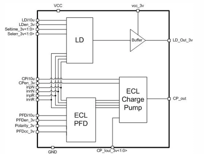
The device consists of phase frequency detector (PFD), charge pump and lock detector (LD).
PFD compares phases of a divided VCO signal and a divided reference oscillator signal. PFD feeds control signal to charge pump at signals mismatch. Charge pump output current forms VCO control voltage.
Lock detector forms output logical “1” at input signals phase coincidence.
The block is fabricated on SMIC CMOS 0.18 um technology.
Phase frequency detector and charge pump
Overview
Key Features
- SMIC CMOS 0.18 um
- Charge pump current control (40 uA, 60 uA, 80 uA, 100 uA)
- Wide range of charge pump output voltage (0.3 V…1.56 V)
- PFD polarity selection
- Lock time selection (64, 128, 216, 512 periods of reference frequency signal)
- Without external components
- Portable to other technologies (upon request)
Block Diagram

Applications
- PLL
- Frequency synthesizer
- Functional signal generator
- Communication devices
Deliverables
- Schematic or NetList
- Abstract model (.lef and .lib files)
- Layout view (optional)
- Behavioral model (Verilog)
- Extracted view (optional)
- GDSII
- DRC, LVS, antenna report
- Test bench with saved configurations (optional)
- Documentation
Technical Specifications
Short description
Phase frequency detector and charge pump
Vendor
Vendor Name
Foundry, Node
SMIC CMOS 0.18 um
Maturity
silicon proven
Availability
Now
Related IPs
- Phase frequency detector and charge pump
- PLL CMOS phase-frequency detector with ECL charge pump
- PLL ECL phase-frequency detector with ECL charge pump
- 0.1 to 25 MHz Phase-frequency detector with charge pump
- 24.84 MHz Phase-frequency detector with charge pump (input amplitude 150…210 mV)
- PLL ECL phase-frequency detector with ECL charge pump