LVDS Rx IP, Silicon Proven in GF 28LPe
Overview
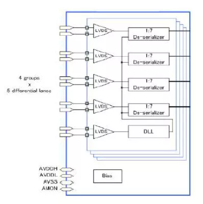
A physical layer IP for LVDS Receiver. This IP consists of 20-lane (4 x 4D1C) LVDS receivers and supports up to 1.5Gbps data rate. The input clock is 25MHz to 150MHz. The serializer is highly integrated and requires no external components. The circuit is designed in a modular fashion and desensitized to process variations. This facilitates process migration, and results in a robust design.
Key Features
- LVDS compliant Rx
- 4 groups of 4-Data, 1-Clock channels
- Each lane/group can be turned on/off individually
- Supports from 168Mbps to 1.5Gbps data rate
- Configurable analog characteristics
- Bias voltage/current
- DLL characteristics
- Testability Internal analog nodes can be observed through a test pad DLL test mode Process
- Supply Voltage 1.8V/0.9V
- Silicon Proven in SMIC 14nm SF+
Block Diagram
Deliverables
- Datasheet
- Integration guideline
- GDSII or Phantom
- GDSII Layer map table
- CDL netlist for LVS
- LEF Verilog behaviour model
- Liberty timing model DRC/LVS/ERC results
Technical Specifications
Short description
LVDS Rx IP, Silicon Proven in GF 28LPe
Vendor
Vendor Name
Foundry, Node
STMicro 28FDSOI
Maturity
In Production
Availability
Immediate
Related IPs
- Bluetooth Dual Mode v5.4 / IEEE 15.4 PHY/RF IP in GF 22nm (Silicon Proven)
- 2.5V GPIO with 2Gbps LVDS RX TX and Analog Cell in GlobalFoundries 65nm LPe
- ONFI 4.1 PHY IP (Silicon Proven in TSMC 12FFC)
- ONFi PHY 4.0 (FPHY+MDLL+SDLL Regulator) (Silicon Proven in TSMC 28HPC+)
- V-by-One/ LVDS Tx IP, Silicon Proven in SMIC 40LL
- GF12 - 0.8V LVDS Rad-Hard Transceiver in GF 12nm