Why ESD Co-Design is Essential for Next-Gen ICs

In the fast-moving world of semiconductor design, electrical overstress (EOS) and electrostatic discharge (ESD) remain stubborn challenges. As silicon nodes shrink and performance demands rise, traditional approaches to ESD protection are reaching their limits. The classic model of sequential ESD design—where the I/O or PHY circuitry is finalized before protection is added—is not only outdated, but also increasingly inefficient.
At Sofics, we’ve been rethinking this paradigm. We believe the future lies in co-design: the collaborative, concurrent development of I/O and ESD protection circuits. It’s a shift that’s already delivering real benefits in performance, area efficiency, and robustness.
At the 2025 RF workshop, a few examples and the main benefits of co-design were presented. This article is a write up of that presentation.

The Problem with the Classic ESD Design Flow
In the traditional design process these are the typical steps:
- A team creates the I/O or PHY circuitry.
- This circuit is then handed off to an ESD team (often external or another group).
- The ESD team is restricted: they can’t touch the I/O design itself.
This rigid separation means ESD circuits must often be overdesigned to accommodate unknowns or limitations in the I/O. The result? Performance suffers, silicon real estate is wasted, and ironically, protection levels may still fall short.
You lose three times:
- Performance loss due to oversized ESD clamps adding parasitic capacitance.
- Larger area from protection circuits that are bulkier than necessary.
- Lower robustness, as internal nodes may not be adequately protected.
Why Co-Design Is the Solution
Modern technologies demand smarter ESD strategies. Consider:
- In deep submicron and SOI technologies, the maximum allowable ESD voltage is decreasing, requiring larger or more effective clamps.
- Internal nodes are becoming more sensitive—and protecting them is essential for full-chip robustness.
- Smart, localized protection can replace the traditional approach, reducing impact on performance and area.
But this requires co-design. ESD protection can’t be an afterthought—it must be built in from the start, with full access to and collaboration on I/O circuits.
Co-Design in Action: Two Examples
1. Overvoltage I/O Protection
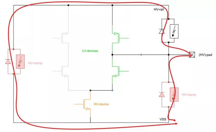
Protecting thin oxide devices against ESD strikes is no small feat. The classic method demands aggressive clamp design. In the example below the HV-pad (right side) is connected to a circuit with a low voltage (thin oxide) PMOS to the high voltage rail and a stack of a low voltage NMOS and high voltage NMOS to the Vss rail. To ensure the low voltage devices are adequately protected the local protection clamps need careful ESD design. A full local protection approach is typically required. This includes a clamp (and reverse diode) between HV pad to HV rail and another clamp between pad and Vss. In the classic method, the ESD designer can only connect diodes and clamps between the rails and the I/O pad. It is not possible to connect anything to internal nodes of the I/O circuit.
Let us look at positive ESD stress on the I/O pad versus the Vss rail. The trigger voltage for the HV-clamp at the bottom (red on figure below) needs to be set high enough to enable high voltage operation. However, at the same time the trigger and clamping voltage should be as low as possible to protect the (green) thin oxide devices. The clamp must protect the stack of the low voltage NMOS and the high voltage NMOS transistors.
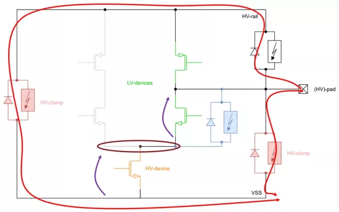
For an improved protection of the thin oxide NMOS transistor during ESD events, the IC designer can add a small local clamp (Blue clamp in the schematic below), in parallel to the NMOS transistor.
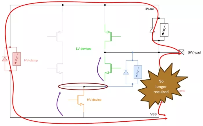
Local protection of internal nodes can dramatically relax the demands on the output clamp. The payoff: smaller clamps, better performance, and lower area cost. In some cases this could even enable the ESD designer to remove the HV clamp entirely.
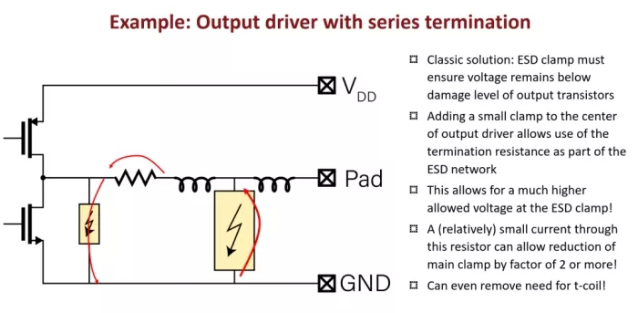
2. Series Termination Output Driver
In this architecture, adding a small clamp at the center node of the driver allows us to leverage the series resistor as part of the ESD protection network. The result?
- The main clamp can be reduced by a factor of two or more.
- In some cases, you can eliminate the need for a T-coil, saving area and simplifying the design.
These are relatively simple illustrations. For more complex circuits, the benefits of co-design become even more pronounced but also require a deep understanding of both I/O and ESD behavior.
Sofics’ Strategic Evolution: More Than Just ESD Protection
To fully realize these benefits, we’re evolving. Sofics is expanding its role from ESD specialist to a complete I/O design partner. This strategic move enables us to:
- Deliver fully optimized, silicon-proven IP.
- Take responsibility for both performance and protection.
- Allow our customers to focus on their core IP, while we ensure interface robustness.
We’re already seeing success in:
- Over-voltage I/Os
- Antenna discharge protection
- High-speed analog drivers and receivers
- Designs integrating T-coils and inductors
Conclusion: ESD Is Not an Afterthought
We made it clear during the recent presentation, “Co-design is essential to maximize performance. ESD cannot be an afterthought.”
The message is obvious: co-design delivers higher performance, more efficient layouts, and more robust circuits. And at Sofics, we are empowering our customers with IP that’s not just protected, but perfected.
Want to Learn More?
If you’re exploring new design nodes, grappling with demanding ESD requirements, or looking for I/O IP that pushes the limits—let’s talk. Our co-design approach might be exactly what your next chip needs.
Related Semiconductor IP
- On-chip ESD/EOS/Latch up protection for advanced and low voltage processes
- On-chip ESD/EOS/Latch up/EMC protection for high voltage and BCD processes
- Robust circuit and interface solutions
- ESD Protection
- High-Speed 3.3V I/O library with 8kV ESD Protection in TSPCo 65nm
Related Blogs
- Why UCIe is Key to Connectivity for Next-Gen AI Chiplets
- Building Secure Chips: Why Hardware Security Assurance Is Now Essential
- The Heart of SiFive is Performance, Intelligence, & Essential
- Why IMG CXT ray tracing is a game-changer for mobile
Latest Blogs
- IDS-Verify™: From Specification to Sign-Off – Automated CSR, Hardware Software Interface and CPU-Peripheral Interface Verification
- RISC-V and GPU Synergy in Practice: A Path Towards High-Performance SoCs from SpacemiT K3
- EDA AI Agents: Intelligent Automation in Semiconductor & PCB Design
- Why Security Can't Exist Without Trust
- Universal Browser Support for JPEG XL: Is Your Hardware Ready for the New Standard?