Signali IP
Filter
Compare
581
IP
from
68
vendors
(1
-
10)
-
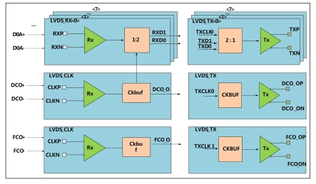
High-speed LVDS (Low-Voltage Differential Signaling) transceiver
- Compatible with ANSI/TIA/EIA 644-1995 LVDS standard
- Multi-channel LVDS transceiver function
- Maximum data transfer rate: 992Mbps (496MHz)
- Typical output voltage: 350mV (100-Ω load)
-
Differential Signaling IO Buffer
- Configurable size of the signal width
- Configurable differential signaling buffer type
-
SMIC 0.18um Reduced Swing Differential Signaling Transmitter
- Process: SMIC0.18 Logic 1P4M/5M/6M (3.3V IO)
- Operating temperature range: -40~125°C
- Supply voltage range: 2.7~3.6V
- Clock frequency: 25~85MHz
-
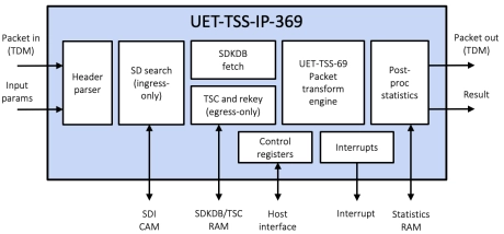
Multi-channel Ultra Ethernet TSS Complete Layer
- The UET-TSS-IP-369 (EIP-369) is an inline, high-performance, multi-channel packet engine that provides the complete TSS layer, bypass/drop and basic crypto processing at rates up to 1.6Tbps.
- The engine is designed for integration into the systems that require TSS processing for one or more ports. The engine is provided as separate ingress and egress data paths.
- The EIP-369 embeds the UET-TSS-IP-69 for the packet transformation.
-
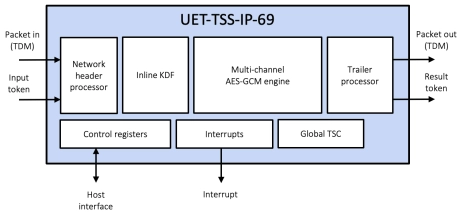
Multi-channel Ultra Ethernet TSS Transform Engine
- The UET-TSS-IP-69 (EIP-69) is a high-performance, multi-channel transform engine that provides the complete TSS packet transformation (including KDF and IP/UDP updates), bypass/drop and basic crypto processing at rates up to 1.6Tbps.
- The engine is designed for integration into the systems that require TSS processing for one or more ports. The engine is provided as separate ingress and egress data paths.
-
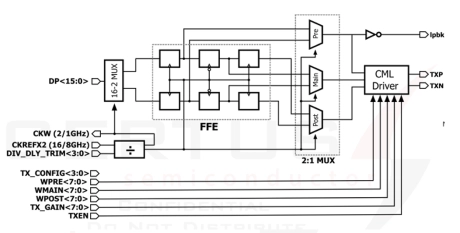
32Gbps SerDes PHY in GF 22nm
- This 32Gbps SerDes PHY is implemented in GlobalFoundries 22FDX CMOS technology and provides a high-performance, protocol-agnostic serial interface for advanced mixed-signal and high-speed digital SoCs.
- The PHY is architected as a modular design consisting of a low-jitter clock multiplier, a half-rate transmitter with digitally programmable feed-forward equalization, and a configurable CTLE-based receiver with digital clock-and-data recovery, supporting both 16 Gbps and 32 Gbps operation.
-
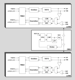
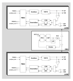
Ultra-Low Latency 32Gbps SerDes IP in TSMC 12nm FFC
- Modular architecture supporting x1 to x16 lanes with a single CMU
- Lane-based PLL architecture supporting flexible, independent data rates from 1.25 to 32Gbps
- Ultra-low latency 2/4/8-bit parallel interface mode for lowest possible latency
-
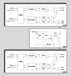
Ultra-Low Latency 32Gbps SerDes IP in TSMC 22nm ULP
- Modular architecture supporting x1 to x16 lanes with a single CMU
- Lane-based PLL architecture supporting flexible, independent data rates from 1.25 to 32Gbps
- Ultra-low latency 2/4/8-bit parallel interface mode for lowest possible latency

-
32Gbps SerDes IP in TSMC 12nm FFC
- Modular architecture supporting x1 to x16 lanes with a single CMU
- Lane-based PLL architecture supporting flexible, independent data rates from 1.25 to 32Gbps
- Configurable low latency parallel data interface for optimal system performance
-
32Gbps SerDes IP in TSMC 22nm ULP
- Modular architecture supporting x1 to x16 lanes with a single CMU
- Lane-based PLL architecture supporting flexible, independent data rates from 1.25 to 32Gbps
- Configurable low latency parallel data interface for optimal system performance