Memory Controller IP
Filter
Compare
1,246
IP
from
126
vendors
(1
-
10)
-
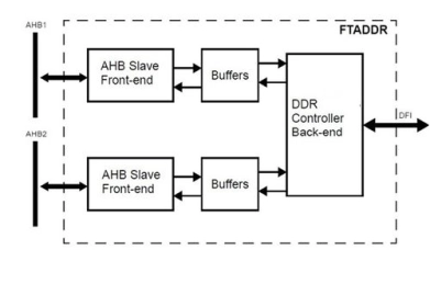
Fault Tolerant DDR2/DDR3/DDR4 Memory controller
- FTADDR is a memory controller for DDR2,DDR3 and DDR4 SDRAM memory devices.
- It uses a strong error correction code to achieve exceptional fault tolerance
-
DDR5 & DDR4 COMBO IO for memory controller PHY, 4800Mbps on TSMC 12nm
- The DDR5&DDR4 COMBO IO is used to transfer the Command/Address/Clk and Data between the memory controller PHY and the DRAM device
- The TX is designed to send information from PHY to DRAM and RX is designed to receive information which is from DRAM._x000D_ It supports DDR5&DDR4 interface
- The DDR5 DQ data rate can be up to 4800Mb/s, and the DDR4 DQ data rate can be up to 3200Mb/s and CA is SDR mode.
-
DDR4 & LPDDR4 COMBO IO for memory controller PHY, 3200Mbps on TSMC 22nm
- The DDR4&LPDDR4 COMBO IO is used to transfer the Command/Address/Clk and Data between the memory controller PHY and the DRAM device
- The TX is designed to send information from PHY to DRAM and RX is designed to receive information which is from DRAM.
-
General Memory Controller
- The GMC (General Memory Controller) includes two memory controllers: The NOR/PSRAM memory controller, The Synchronous DRAM (SDRAM/Mobile LPSDR SDRAM) controller
-
PSRAM Memory Controller IP
- DFSPI – SPI FLASH Controller with Execute in place – XIP (SINGLE, DUAL and QUAD SPI Bus Controller with DDR / DTR support and optional AES Encryption) + … NOR & NAND Flash Memory Support
-
HYPERBUS™ Memory Controller
- The HyperBus™ Memory Controller IP Core is a high-speed, fully configurable SPI master/slave solution, designed for seamless integration into modern SoC and FPGA architectures.
- Building on the proven DFSPI core, this IP bridges easily to APB, AHB, and AXI buses, supporting SINGLE, DUAL, QUAD, and OCTAL SPI modes for maximum design flexibility.
-
NAND Memory Controller
- The NAND memory controller IP core is compliant with the ONFI standard working on asynchronous mode.
- This core also supports error correction on the fly without any processor intervention. Up to 8 memory chips can be accessed on the same bus with write speed of 100Mbps and read speeds of 120Mbps.
-
High-Performance Memory Controller II SDRAM Intel® FPGA IP Core
- The High-Performance Memory Controller II SDRAM Intel FPGA IP core handles the complex aspects of using DDR, DDR2, and DDR3 SDRAM at speeds up to 933 MHz
- The intellectual property (IP) core initializes the memory devices, manages SDRAM banks, translates read-and-write requests from the local interface into all the necessary SDRAM command signals, and performs command and data reordering.

-
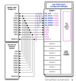
xSPI Multiple Bus Memory Controller
- SLL’s unified xSPI Multiple Bus Memory Controller IP supports the widest range of JEDEC xSPI and xSPI-like NOR Flash and PSRAM memories (JEDEC xSPI Profile 1.0 and 2.0, HyperBus 1.0, 2.0 and 3.0, OctaBus and Xccela Bus) that are available now from many memory vendors.
- JEDEC xSPI and xSPI-like memories offer good performance with lower hardware and power costs. Memory device variants offer up to 512 Mbit PSRAM, up to 2 Gigabit NOR Flash, up to 250 MHz DDR clock speeds, with x4, x8 and x16 data path widths, and a wide range of package options including 4mm x 4mm BGA49 and tiny WLCSP footprints. Some PRSAM devices are now also available with internal ECC.
-
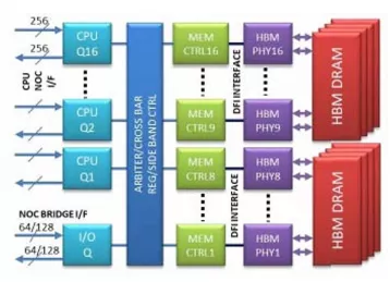
HBM Memory Controller
- Low latency, high bandwidth
- Supports HBM or DDRx memory types
- 16 parallel access channels
- Multi, independent internal queues