Hi-Speed USB IP
Filter
Compare
26
IP
from
4
vendors
(1
-
10)
-
USB 2.0 Hi-Speed OTG Controller version 4 with Active Clock Gating to save active power
- Configuration options to maximize performance and minimize CPU interrupts
- Flexible parameters enable easy integration into low and high-latency systems
- Transfer- or transaction-based processing of USB data based on system requirements
- Configurable data buffering options to fine-tune performance/ area trade-offs
-
USB 2.0 Hi-Speed OTG Controller Subsystem w/AHB Interface Supporting HSIC (config. as Device only or Full Speed only)
- Configuration options to maximize performance and minimize CPU interrupts
- Flexible parameters enable easy integration into low and high-latency systems
- Transfer- or transaction-based processing of USB data based on system requirements
- Configurable data buffering options to fine-tune performance/ area trade-offs

-
USB 2.0 OTG Dual Role Device (DRD) Controller
- Compliant with OTG Supplement Rev. 1.0a
- USB 2.0 Compliant
- Supports 480 Mbit/s (HS), 12 Mbit/s (FS), and 1.5 Mbit/s (LS)
- Supports Session Request Protocol (SRP) and Host Negotiation Protocol (HNP)
-
USB 2.0 Device Controller version 4 with Active Clock Gating to save active power
- Configuration options to maximize performance and minimize CPU interrupts
- Flexible parameters enable easy integration into low and high-latency systems
- Transfer- or transaction-based processing of USB data based on system requirements
- Configurable data buffering options to fine-tune performance/ area trade-offs

-
USB 2.0 femtoPHY - TSMC 40ULP25 x1, OTG, Type-C
- Saves on average $0.03 per die with 50% smaller USB silicon area than competing solutions
- Extends battery life with near 0W standby power consumption and 30% lower active power
- Saves months of implementation and verification effort with simplified configuration options
- Supports USB 2.0 Hi-Speed, Full Speed, and Low Speed

-
USB 2.0 picoPHY in GF (40nm, 28nm)
- Complete mixed-signal physical layer for single-chip USB 2.0 OTG and non-OTG applications
- Small PHY macro area
- Low power
- Advanced power management features, including support for power supply gating, supply scaling, ultra-low standby current support, and power management unit (PMU) interrupt support
-
USB 2.0 nanoPHY in GF (55nm)
- Complete mixed-signal physical layer for single-chip USB 2.0 OTG and non-OTG applications
- Low power: <100mW (during HS packet transmission)
- Small area: ~ 0.6mm2
- High yield—Architecture designed to improve key operating margins by having less sensitivity to variations due to foundry process, chip and board parasitics, and process device model variations
-
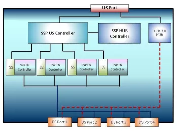
Super-Speed Plus USB 3.2 Hub Controller
- Supports two lanes or one lane - easily configurable
- Number of downstream ports can be easily selected
- Complies with USB 3.2 standard for Super-Speed Plus(10Gbps),Super-Speed(5.0 Gbps), Hi-Speed (480 Mbps), Full-Speed (12 Mbps) and Low-Speed (1.5 Mbps).
- Backward compatible with USB2.0 devices and hubs and the type A connectors.
-
USB 2.0 Digital Controller IP
- Fully supports Hi-Speed (480 Mbps), Full Speed (12 Mbps), and Low Speed (1.5 Mbps) (USB 2.0 Speeds) specifications
- Configurable root hub supports 1 to 15 downstream ports
- 60MHz or 30MHz input clock, and 48MHz and 12MHz input clocks
- ULPI and UTMI+ interfaces for rapid PHY integration
-
USB 2.0 picoPHY in UMC (40nm, 28nm)
- Complete mixed-signal physical layer for single-chip USB 2.0 OTG and non-OTG applications
- Small PHY macro area
- Low power
- Advanced power management features, including support for power supply gating, supply scaling, ultra-low standby current support, and power management unit (PMU) interrupt support