GDDR6 PHY TSMC 7nm IP
Filter
Compare
15
IP
from
5
vendors
(1
-
10)
-
GDDR6 PHY IP on GF 12nm LPP
- The UniIC GDDR6 PHY,subsequently referred to as the UNIIC_GD6PHY, is designed for performance and power efficiency, its target is to deliver industry-leading data rates of up to 12Gbps/13Gbps/14Gbps and is compatible with JEDEC standard JEDEC250 and DFI 3.1
- The UNIIC_GD6PHY is used to transfer the Command/Address and Datas between the memory controller and the GDDR6 DRAM device; _x000D_ The UNIIC_GD6PHY is available in Global Foundries FinFET 12LPP technology
- The UNIIC_GD6PHY is fully documented and comes with a comprehensive set of deliverables for ease of system modeling and integration.
-
GDDR6 PHY
- Single configuration supports one GDDR6 device per channel (coplanar) or two GDDR6 devices per channel (clamshell)
- DFI PHY Independent Mode for initialization and training
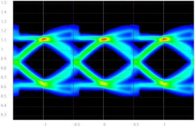
- Adaptive and continuous timing recovery
- Internal and external datapath loop-back modes
- Transmit crosstalk cancelation of immediate neighbors
- Per-bit DFE, CTLE, and FFE equalization
-
GDDR6 PHY IP for 12nm
- JEDEC JESD250 compliant GDDR6 support
- X16 mode, X8 mode, and pseudo-channel mode
- Low frequency RDQS mode support

-
LPDDR5X/5/4X/4 combo PHY at 12nm
- Compliant with JEDEC JESD209-5C for LPDDR5x/5/4x/4 with PHY standards
- Delivering up to 8533Mbps
- DFI 5.1 specification PHY Interface Compliant
- Support up to 4 ranks
- Multiple frequency states

-
LPDDR5X/5/4X/4 PHY for 16nm
- Compliant with JEDEC standards for LPDDR5X/5/4X/4 with PHY standards
- DFI 5.0 Interface Compliant
- Supports up to 4 ranks
- Multiple frequency states
-
LPDDR PHY
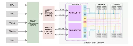
- Application-optimized configurations for fast time to delivery and lower risk
- Low-power VDD idle, VDD light sleep, and power-efficient clocking in low-speed modes
- I/O pads with impedance calibration logic and data-retention capability
- Fine-grain custom delay cell for delay tuning
- Internal and external datapath loop-back modes
- RX and TX equalization for heavily loaded systems
- Programmable per-bit (PVT compensated) deskew on read and write datapaths
-
LPDDR5X/5/4X/4 PHY IP for 12nm
- Compliant with JEDEC standards for LPDDR5X/5/4X/4 with PHY standards
- DFI 5.0 Interface Compliant
- Supports up to 4 ranks
- Multiple frequency states

-
HBM3 PHY IP at 7/6nm
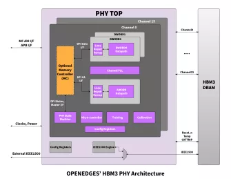
- Compliant with JEDEC JESD238 HBM3
- DFI5.1-based interface with memory controller
- Compliant with ESD requirements
- Supports up to 16-bit independent and asynchronous channel
-
GDDR6X/6 Combo PHY & Controller
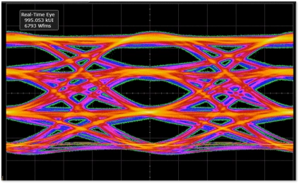
- The GDDR6X/6 PHY is fully compliant with the JEDEC GDDR6X/6 standard, supporting data rates of up to 20Gbps per pin for PAM2 GDDR6 mode and 24Gbps for PAM4 GDDR6X mode
- The GDDR6X/6 interface supports 2 channels, each with 16 bits for a total data width of 32 bits per memory device
- With a maximum speed of 20/24Gbps per pin, The GDDR6X/6 Combo PHY delivers a peak bandwidth of up to 80GB/s or 96GB/s per memory device
-
GDDR6 Controller
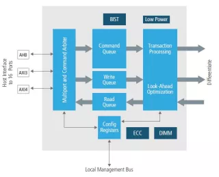
- In-line SEC/DED ECC
- Supports advanced RAS features including error scrubbing, parity, etc.
- Compatible with GDDR6 devices compliant to JESD250b
- Single and multi-port host options for Arm® AMBA®4, AMBA 3 AXI, and low-latency Denali interfaces
- QoS features allow command prioritization
- Flexible paging policy
