DDR4 SDRAM PHY IP
Filter
Compare
91
IP
from
7
vendors
(1
-
10)
-
DDR4 PHY - TSMC N7
- Supports JEDEC standard DDR4, DDR3, and DDR3L SDRAMs
- High-performance DDR PHY supporting data rates up to 3200 Mbps
- Compatible with JEDEC compliant DDR3/4 UDIMMs and RDIMMs as well as DDR4 LRDIMMs
- Supports up to 16 logical ranks for high capacity memory requirements
-
DDR4 PHY
- ? DDR4, LPDDR3, LPDDR2, DDR3, DDR3L, and DDR3U operation
- ?1.2V DDR4 SDRAMs operating at data rates up to 2400Mbps
- ?1.2V LPDDR2 SDRAMs operating at data rates up to 1066Mbps
- ?1.35V DDR3L SDRAMs operating at data rates up to 1866Mbps
-
DDR4/ DDR3 Combo PHY IP - 2400Mbps (Silicon Proven in UMC 28HPC+)
- Supports DDR4/DDR3 SDRAM
- DDR4 JEDEC standard 1.2v I/O (POD_12 I/O)
- DDR3 JEDEC standard 1.5v I/O (SSTL_15-compatible)
- 16 bits width, Single Channel DDR4/DDR3 SDRAM Interface.
-
DDR4/ DDR3/ DDR3L Combo PHY IP - 1600Mpbs (Silicon Proven in TSMC 28HPC+)
- Supported DRAM type: DDR3/DDR3L/DDR4
- Maximum controller clock frequency of 400MHz resulting in maximum DRAM data rate of 1600Mbps
- Interface: SSTL15/SSTL135/POD12
- Data path width scales in 16-bit increment
-
DDR4/LPDDR4 PHY Interface
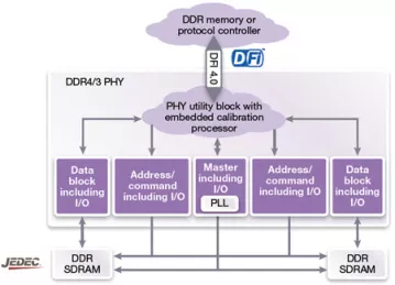
- The DDR PHY IP is a combination of hard macro, I/O Pad and synthesizable RTL to provide a physical interface to JEDEC standard DDR3/DDR4 SDRAM memories.
- The synthesizable RTL (ddr_phy_top) provides control functions such as initialization, SDRAM interface training, impedance calibration and programmable configuration controls.
-
MRDIMM DDR5 & DDR5/4 PHY & Controller
- The DDR IP Mixed-Signal MRDIMM DDR5 PHY and DDR5/4 Combo PHY provide turnkey physical interface solutions for ICs requiring access to JEDEC compatible SDRAM or MRDIMM/ RDIMM/ LRDIMM/ UDIMM DDR5 devices
- It is optimized for low-power and high-speed applications with robust timing and small silicon area
- It supports all JEDEC DDR5/4 SDRAM components in the market
-
DDR4 multiPHY SP - SS 14LPP
- Support for JEDEC standard DDR4, DDR3, LPDDR2, and LPDDR3 SDRAMs
- Scalable architecture that supports data rates up to DDR4-2667
- Support for DIMMs
- Delivery of product as a hardened mixed-signal macrocell component allows precise control of timing critical delay and skew paths

-
DDR4 multiPHY - UMC 28HPC18
- Support for JEDEC standard DDR4, DDR3, LPDDR2, and LPDDR3 SDRAMs
- Scalable architecture that supports data rates up to DDR4-2667
- Support for DIMMs
- Delivery of product as a hardened mixed-signal macrocell component allows precise control of timing critical delay and skew paths

-
DDR4 multiPHY - TSMC 28HPC+18
- Support for JEDEC standard DDR4, DDR3, LPDDR2, and LPDDR3 SDRAMs
- Scalable architecture that supports data rates up to DDR4-2667
- Support for DIMMs
- Delivery of product as a hardened mixed-signal macrocell component allows precise control of timing critical delay and skew paths

-
DDR4/3 PHY - TSMC 16FFC
- Supports JEDEC standard DDR4, DDR3, and DDR3L SDRAMs
- High-performance DDR PHY supporting data rates up to 3200 Mbps
- Compatible with JEDEC compliant DDR3/4 UDIMMs and RDIMMs as well as DDR4 LRDIMMs
- Supports up to 16 logical ranks for high capacity memory requirements
