DDR4 DRAM Memory Controller IP
Filter
Compare
73
IP
from
8
vendors
(1
-
10)
-
DDR4 / DDR3/ DDR3L / LPDDR4 Memory Controller IP optimized for low latency
- Support DDR3 / DDR3L / DDR4/ 3DS DDR4/ LPDDR4 / MRAM
- Support x8/x16/x32 DRAM data bus configuration (programmable)
- Support Multi-Ranks DRAM configuration
- DDR base on DFI spec 4.0 compliant.
-
DDR5 & DDR4 COMBO IO for memory controller PHY, 4800Mbps on TSMC 12nm
- The DDR5&DDR4 COMBO IO is used to transfer the Command/Address/Clk and Data between the memory controller PHY and the DRAM device
- The TX is designed to send information from PHY to DRAM and RX is designed to receive information which is from DRAM._x000D_ It supports DDR5&DDR4 interface
- The DDR5 DQ data rate can be up to 4800Mb/s, and the DDR4 DQ data rate can be up to 3200Mb/s and CA is SDR mode.
-
DDR4 & LPDDR4 COMBO IO for memory controller PHY, 3200Mbps on TSMC 22nm
- The DDR4&LPDDR4 COMBO IO is used to transfer the Command/Address/Clk and Data between the memory controller PHY and the DRAM device
- The TX is designed to send information from PHY to DRAM and RX is designed to receive information which is from DRAM.
-
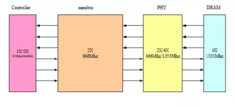
DDR 4/3 Memory Controller IP - 2400MHz
- Support s DDR 4 /DDR3 SDRAM
- 16 bit s width , Single Channel DDR 4 /DDR3 SDRAM Interface .
- 16 bits for per channel, could support 2 x8 bits DDR3, but could not support 2 x8 bits DDR4.
- Memory Clock up to 6 66 MHz, DFI Clock up to 666 MHz .
-
DDR3L/ LPDDR4/ DDR4 PHY IP - 1866Mbps (Silicon Proven in UMC 28HPC+)
- Supported DRAM type: DDR3L/DDR4/LPDDR4
- Maximum controller clock frequency of 400MHz resulting in maximum DRAM data rate of 1866Mbps
- Interface: SSTL135/POD12/LVSTL
- Data path width scales in 32-bit increment

-
-
DDR4 IO for memory PHY, 3200Mbps on SMIC 40nm
- The DDR4 IO is used to transfer the Command/Address/Clk and Data between the memory controller PHY and the DRAM device
- The TX is designed to send information from PHY to DRAM and RX is designed to receive information which is from DRAM.
-
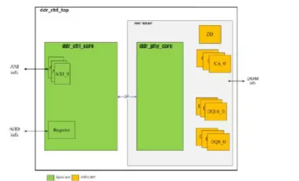
DDR4/LPDDR4 Controller
- On the host side, DDR4/LPDDR4 Controller supports up to 16 AMBA4 AXI. The configuration registers are programmed through the APB interface.
- On the DFI side, DDR4/LPDDR4 Controller supports for intergration with DFI4.0-compliant PHY.
-
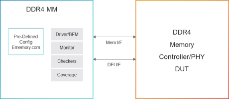
Simulation VIP for DDR4
- Data Width, Density
- 4, 8, and 16. 2 Gb to 16 Gb
- Speed
- 1600, 1866, 2133, 2400, 2666, and 3200
-
DDR4 Multi-modal PHY - GLOBALFOUNDRIES 12nm
- PLL-based clocking with internal clock alignment to the parallel clock on the memory controller interface
- Autonomous initialization
- Support for x72 bit channel
- Support for multiple DRAM widths (x4, x8, x16, x32)