DDR2 SDRAM IP
Filter
Compare
39
IP
from
17
vendors
(1
-
10)
-
DDR and DDR2 SDRAM Controller with ALTMEMPHY Intel® FPGA IP
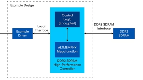
- The DDR and DDR2 SDRAM Controller with ALTMEMPHY Intel FPGA Intellectual Property (IP) provides simplified interfaces to industry-standard DDR SDRAM and DDR2 SDRAM
- The DDR and DDR2 SDRAM Controller with ALTMEMPHY Intel FPGA IP core work in conjunction with the ALTMEMPHY physical interface IP function
- The controllers offer a half-rate interface and a full-rate interface to the customer application logic
- For exact device support, please refer to the user guide.
-
DDR and DDR2 SDRAM Controller Intel® FPGA IP Core
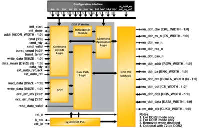
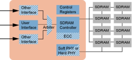
- The DDR and DDR2 SDRAM controllers handle the complex aspects of using DDR and DDR2 SDRAM—initializing the memory devices, managing SDRAM banks, and keeping the devices refreshed at appropriate intervals
- The controllers translate read-and-write requests from the local interface into all the necessary SDRAM command signals.
-
DDR2 SDRAM Controller - Pipelined
- Interfaces to Industry Standard DDR2 SDRAM
- High-Performance DDR2 533/400/333/266/200/133 operation
- Programmable Burst Lengths of 4 or 8
- Programmable CAS Latency of 3, 4, 5 or 6 Cycles
-
DDR2 SDRAM Controller
- Supports industrial standard Double Data Rate (DDR) and Double Date Rate2 (DDR2) SDRAM from 64Mbit to 2Gbit device sizes.
- Page hit detection to support multiple column accesses within the same row.
- Pipeline access enables continuous data bursting and hidden active commands, even in the case of page misses.
- Issue precharge, active and read/write commands to multiple banks at the same time.
-
DDR2 SDRAM Controller IP
- Supports DDR2 protocol standard JESD79-2F Specification.
- Compliant with DFI-version 2.0 or higher Specification.
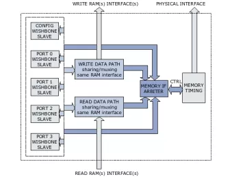
- Supports all the DDR2 commands as per the specs. Supports up to 16 AXI ports with data width upto 512 bits.
- Supports controllable outstanding transactions for AXI write and read channels
-
-
High-Performance Memory Controller II SDRAM Intel® FPGA IP Core
- The High-Performance Memory Controller II SDRAM Intel FPGA IP core handles the complex aspects of using DDR, DDR2, and DDR3 SDRAM at speeds up to 933 MHz
- The intellectual property (IP) core initializes the memory devices, manages SDRAM banks, translates read-and-write requests from the local interface into all the necessary SDRAM command signals, and performs command and data reordering.

-
Performance Enhanced version of uMCTL2 supporting DDR4, DDR3, DDR2, LPDDR4, LPDDR3 and LPDDR2 for Automotive
- Select a complete multi-ported Enhanced Universal DDR Memory Controller offering 1 to 16 host ports, or join a third-party scheduler to a single-port Enhanced Universal Protocol Controller
- Support for JEDEC standard DDR2, DDR3, DDR4, LPDDR/Mobile DDR, LPDDR2, LPDDR3, and LPDDR4 SDRAMs
- Compatible with all Synopsys DDR PHYs (excluding DDR2/DDR PHYs) using DFI-compliant interfaces

-
Performance Enhanced version of DDR Enhanced Memory Ctl (uMCTL2) supporting DDR4, DDR3, DDR2, LPDDR4, LPDDR3, and LPDDR2
- Select a complete multi-ported Enhanced Universal DDR Memory Controller offering 1 to 16 host ports, or join a third-party scheduler to a single-port Enhanced Universal Protocol Controller
- Support for JEDEC standard DDR2, DDR3, DDR4, LPDDR/Mobile DDR, LPDDR2, LPDDR3, and LPDDR4 SDRAMs
- Compatible with all Synopsys DDR PHYs (excluding DDR2/DDR PHYs) using DFI-compliant interfaces

-
DDR Enhanced Protocol Controller (uPCTL2) supporting DDR4, DDR3, DDR2, LPDDR4, LPDDR3, and LPDDR2
- Select a complete multi-ported Enhanced Universal DDR Memory Controller offering 1 to 16 host ports, or join a third-party scheduler to a single-port Enhanced Universal Protocol Controller
- Support for JEDEC standard DDR2, DDR3, DDR4, LPDDR/Mobile DDR, LPDDR2, LPDDR3, and LPDDR4 SDRAMs
- Compatible with all Synopsys DDR PHYs (excluding DDR2/DDR PHYs) using DFI-compliant interfaces
