Cadence IP
Filter
Compare
210
IP
from
16
vendors
(1
-
10)
-
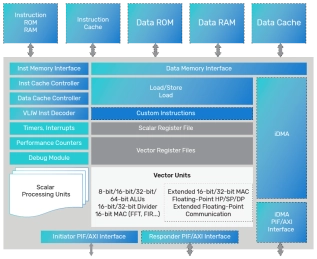
Tensilica ConnX 120 DSP
- Certified ISO 26262:2018 ASIL-compliant
- VLIW parallelism issuing multiple concurrent operations per cycle
- 256-bit SIMD
- Up to 64 MAC
-
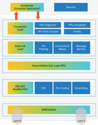
UALink Controller
- The UALink Controller, part of Cadence’s verified UALink IP subsystem, delivers ultra-low latency and high-bandwidth interconnects that enable seamless scale-up connectivity between AI accelerators. I
- t supports memory semantics for read, write, and atomic operations, ensuring fast, coherent data handling across workloads. UALink IP provides a scalable, future-ready solution for next-generation AI infrastructure.
-
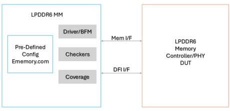
Simulation VIP for LPDDR6
- This Verification IP (VIP) is intended for modeling the upcoming JEDEC Low-Power Memory Device, LPDDR6 design specification.
- It provides a mature, highly capable compliance verification solution that supports simulation, formal analysis, and hardware acceleration platforms, making it applicable to intellectual property (IP), system-on-chip (SoC), and system-level verification.
-
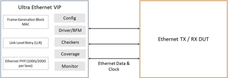
Simulation VIP for Ethernet UEC
- Support testbench language interfaces for SystemVerilog, UVM, OVM, e, and SystemC
- Callbacks access at multiple TX and RX queue points for scoreboarding, data manipulation, and error injection
- Transaction Tracker: Configurable tracking of all the transactions on the channels
-
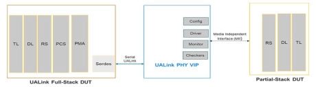
Simulation VIP for UALink
- The Ultra Accelerator Link (UALink) Verification IP (VIP) provides a complete bus functional model (BFM) with integrated automatic protocol checks for physical layer in addition to Media Independent Interface (MII).
- Designed for easy integration in testbenches at IP, SoC, and system levels, the VIP helps engineers reduce time to first test, accelerate verification closure, and ensure end-product quality.
-
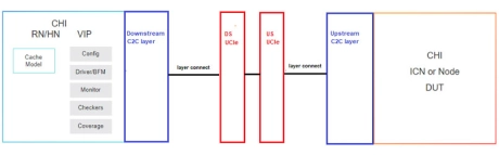
Simulation VIP for AMBA CHI-C2C
- Incorporating the latest protocol updates, the Cadence Verification IP for CHI-C2C provides a complete bus functional model (BFM), integrated automatic protocol checks, and a coverage model.
- Designed for easy integration in testbenches at IP, systems with multiple CPUs, accelerators, or other device chiplets, the VIP for CHI-C2C provides a highly capable compliance verification solution that supports simulation, formal analysis, and hardware acceleration platforms.
-
224G SerDes PHY and controller for UALink for AI systems
- UALink, the standard for AI accelerator interconnects, facilitates this scalability by providing low-latency, high-bandwidth communication.
- As a member of the UALink Consortium, Cadence offers verified UALink IP subsystems, including controllers and silicon-proven PHYs, optimized for robust performance in both short and long-reach applications and delivering industry-leading power, performance, and area (PPA).
-
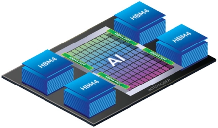
HBM4E PHY and controller
- Advanced clocking architecture minimizes clock jitter
- DFI PHY Independent Mode for initialization and training
- IEEE 1500 interface, memory BIST feature, and loop-back function
- Supports lane repair
-
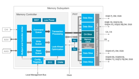
DDR5 MRDIMM PHY and Controller
- The DDR5 12.8Gbps MRDIMM Gen2 PHY and controller memory IP system solutions double the performance of DDR5 DRAM.
- The DDDR5 12.8Gbps design and architecture address the need for greater memory bandwidth to accommodate unprecedented AI processing demands in enterprise and data center applications, including AI in the cloud.
-
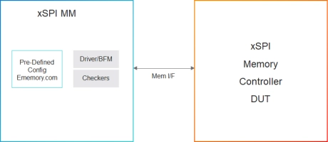
Simulation VIP for xSPI
- xSPI Profile 1
- SPI (Read Zero Latency), DUAL (1-1-2, 1-2-2), Quad (As per JESD251-A1), and Octal modes Data Rate: STR and DTR
- Modes
- SPI-STR (1S-1S-1S), QUAD-STR (4S-4S-4S), OCTAL-STR(8S-8S-8S), and OCTAL-DTR (8D-8D-8D) modes