AHB compliant Cache controller IP
Filter
Compare
26
IP
from
6
vendors
(1
-
10)
-
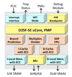
64-bit CPU Core with Level-2 Cache Controller
- AndeStar™ V5 Instruction Set Architecture (ISA), compliant to RISC-V technology
- Floating point extensions
- DSP/SIMD ISA to boost the performance of voice, audio, image and signal processing
- Andes extensions, architected for performance and functionality enhancements
- Separately licensable Andes Custom Extension™ (ACE) for customized acceleration

-
ONFI 2 NAND Flash Controller IP Compliant to JEDEC
- The ONFI 2.3 NAND Flash Controller IP Core is a full-featured, easy to use, synthesizable core, easily integrated into any SoC or FPGA development.
- Designed to support both SLC and MLC flash memories, ONFI 2.3 NAND controller IP is flexible in use and easy in implementation.

-
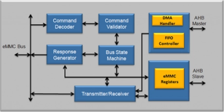
eMMC 4.51 Device Controller IP
- Compliant to JEDEC JESD84-B45 eMMC 4.51 spec
- Packed commands for faster processing
- Supports cache control mechanism
- Supports eMMC4.51 Security Protocol Commands
-
MIPI LLI Controller
- The LLI Controller connects two chips together to create a single “virtual chip”, with both chips sharing the same memory.
- This is achieved by the low latency from the “companion” chip to the memory interface of the host chip.
-
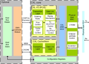
CXL CONTROLLER IIP
- Compliant with CXL 1.0/1.1 Specifications
- Supports Native PCIe mode and below features as defined in the PCIe specification
- PCIE Express specs 1.0/2.0/3.0/4.0/5.0
- PIPE interface
-
32-bit CPU IP core - ISO 26262 Automotive Functional Safety Compliant
- 32-bit CPU IP core that supports ISO 26262 ASIL B level functional safety for automotive applications
-
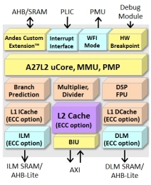
Compact High-Speed 32-bit CPU Core with Level-2 Cache
- AndeStar™ V5 Instruction Set Architecture (ISA), compliant to RISC-V technology
- Floating point extensions
- DSP/SIMD ISA to boost the performance of voice, audio, image and signal processing
- Andes extensions, architected for performance and functionality enhancements
-
32-Bit SPARC V8 Processor
- SPARC V8 instruction set with V8e extensions and compare-and-swap
- Advanced 7-stage dual-issue pipeline
-
64-bit Multiprocessor with Level-2 Cache-Coherence
- Symmetric multiprocessing up to 4 cores
- Level-2 cache and cache coherence support
- AndeStar™ V5 Instruction Set Architecture (ISA). Compliant to RISC-V ISA IMACFDN, with Andes performance/functionality extensions
- Floating point extension

-
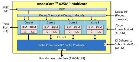
32-bit Multiprocessor with Level-2 Cache-Coherence
- AndesCore™ A25MP 32-bit multicore CPU IP is based on AndeStar™ V5 architecture.
- It supports RISC-V standard ‘IMAC-FD’ extensions, Andes contributed DSP/SIMD 'P' extension (draft), user-level interrupt 'N' extension, and Andes performance/functionality enhancements such as instructions for faster memory accesses, faster branch handling, and Andes Custom Extension™ (ACE) to add user defined instructions.