Memory Controller/PHY IP for TSMC
Welcome to the ultimate
Memory Controller/PHY IP
for
TSMC
hub! Explore our vast directory of
Memory Controller/PHY IP
for
TSMC
All offers in
Memory Controller/PHY IP
for
TSMC
Filter
Compare
39
Memory Controller/PHY IP
for
TSMC
from
7
vendors
(1
-
10)
Filter:
- 7nm
-
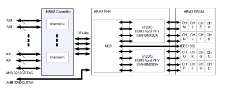
TSMC CLN7FF HBM3 PHY
- IGAHBMX03A is a HBM3 (High Bandwidth Memory) PHY IP compliant to the JEDEC HBM3 DRAM Specification Rev 0.95.
- Built on TSMC 7nm process node, it supports data rate up to 7200 Mbps per data pin with DFI 1:4 clock frequency ratio (controller clock : WCK = 1:4).
-
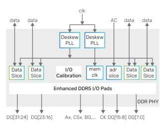
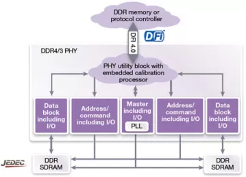
DDR5/4 PHY for TSMC 7nm
- Application optimized configurations for fast time to delivery and lower risk
- Memory controller interface complies with DFI standards up to 5.0
- Internal and external datapath loop-back modes
- Per-bit deskew on read and write datapath
-
SD/eMMC - TSMC 7FF, North/South Poly Orientation
- Compliant with eMMC 5.1 HS400, SD 6.0 SDR104, DDR50, JESD8-7a (1.2V/1.8V) and JESD8c.01 (3.3V)
- Fully integrated hard macro with high speed IOs and DLL/delay lines
- Fine resolution DLL/delay lines for HS400 strobe and HS200/SDR104 auto-tuning
- Easy to integrate with the highly optimized Synopsys SD/eMMC Host Controller IP, providing a complete low risk solution
-
HBM2E PHY V2 - TSMC 7FF18
- Complete HBM2/HBM2E IP solution, including PHY, controller and verification IP, reduces integration risk while minimizing time-to-market
- 2.5D interposer expertise and reference designs
- Supports 2.5D-based JEDEC standard HBM2/HBM2E SDRAMs with data rates up to 3200 Mbps

-
HBM2E PHY V2 (Hard 1) - TSMC 7FF18
- Complete HBM2/HBM2E IP solution, including PHY, controller and verification IP, reduces integration risk while minimizing time-to-market
- 2.5D interposer expertise and reference designs
- Supports 2.5D-based JEDEC standard HBM2/HBM2E SDRAMs with data rates up to 3200 Mbps
-
LPDDR4X multiPHY - TSMC N7
- Supports JEDEC standard LPDDR4X, LPDDR4, LPDDR3, DDR4, DDR3, and DDR3L (1.35V DDR3) SDRAMs
- Support for data rates up to 4,267 Mbps (process dependent)
- Designed for rapid integration with Synopsys Enhanced Universal DDR Memory/Protocol Controllers (uMCTL2/uPCTL2) for a complete DDR interface solution
- PHY independent, firmware-based training using an embedded calibration processor

-
DDR4 PHY - TSMC N7
- Supports JEDEC standard DDR4, DDR3, and DDR3L SDRAMs
- High-performance DDR PHY supporting data rates up to 3200 Mbps
- Compatible with JEDEC compliant DDR3/4 UDIMMs and RDIMMs as well as DDR4 LRDIMMs
- Supports up to 16 logical ranks for high capacity memory requirements
-
LPDDR5/4/4X PHY - TSMC N7 for Automotive, ASIL B Random, AEC-Q100 Grade 2
- Supports JEDEC standard LPDDR5X, LPDDR5, LPDDR4 and LPDDR4X SDRAMs
- Support for data rates up to 6400 Mbps
- Designed for rapid integration with Synopsys’ LPDDR5/4/4X controller for a complete DDR interface solution
- DFI 5.0 controller interface

-
LPDDR5/4/4X PHY - TSMC N7
- Supports JEDEC standard LPDDR5X, LPDDR5, LPDDR4 and LPDDR4X SDRAMs
- Support for data rates up to 6400 Mbps
- Designed for rapid integration with Synopsys’ LPDDR5/4/4X controller for a complete DDR interface solution
- DFI 5.0 controller interface

-
DDR5/4 PHY V2 - TSMC N7
- Supports JEDEC standard DDR5 and DDR4 SDRAMs
- High-performance DDR PHY supporting data rates up to 8400 Mbps
- PHY independent, firmware-based training using an embedded calibration processor
- Supports up to 4 trained states/ frequencies with <3μs switching time
