General-Purpose I/O (GPIO) IP for GLOBALFOUNDRIES
Welcome to the ultimate
General-Purpose I/O (GPIO) IP
for
GLOBALFOUNDRIES
hub! Explore our vast directory of
General-Purpose I/O (GPIO) IP
for
GLOBALFOUNDRIES
All offers in
General-Purpose I/O (GPIO) IP
for
GLOBALFOUNDRIES
Filter
Compare
30
General-Purpose I/O (GPIO) IP
for
GLOBALFOUNDRIES
from
5
vendors
(1
-
10)
-
1.8V/3.3V GPIO With I2C Compliant ODIO in GF 55nm
- This I/O Library, developed on GlobalFoundries 55nm CMOS, delivers a complete suite of digital and analog I/O solutions with robust 2 kV HBM / 500 V CDM ESD protection and latch-up immunity.
- The library includes 1.8/3.3 V GPIOs supporting GMII and LVCMOS standards, I2C-compliant ODIOs, and flexible analog I/Os (ANA/DANA) with integrated ESD.
-
IO Library - GLOBALFOUNDRIES 22FDX
- Library contains approx. 60 IO cells
- Support for all metal-stacks of 22FDX®
- Low voltage cells with nominal core voltages down to 0.4 V for glue-less interfacing to ULV Racyics® ABX digital standard cell domains
- Low leakage cells for ultra low power always-on domain usage
-
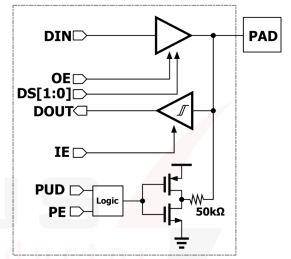
1.8V and 3.3V Radiation-Hardened GPIO with Optimized LDO in GF 12nm
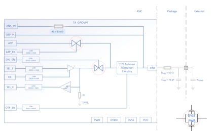
- A radiation-hardened GlobalFoundries 12nm LP/LP+ Flip-Chip IO library with both 1.8V and 3.3V GPIO, fail-safe GPI, analog cell, and associated ESD. Also features an LDO optimized for use with 3.3V GPIO.
- This radiation-hardened, by design, library features both a 1.8 and 3.3V GPIO with multiple drive strengths of 2mA, 4mA, 8mA, and 16mA, along with a full-speed output enable function.
-
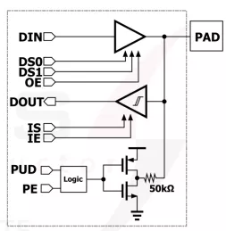
3.3V I/O Library with I2C compliant ODIO IN GF 65/55nm
- A 3.3V wire-bond I/O library, a 1.2V ODIO and 5V tolerant ODIO.
- This library is a production-quality, silicon-proven I/O library in GlobalFoundries 65/55nm technology.
- The library offers a 3.3V GPIO with two selectable inputs, slew rate control, and an optional active tri-state, as well as a GPIO with an ultra-wide supply range and an optional glitch filter.
-
1.5V to 3.3V GPIO with Tri-State Output Driver in GF 180nm
- A GlobalFoundries 180nm BCD Lite Wirebond GPIO library with tri-state out- put driver, schmitt trigger receiver and associated ESD.
- This silicon-proven, wirebond library in GlobalFoundries 180nm BCD lite is a specialty I/O similar to Soundwire.
- Featuring a 1.5V to 3.3V GPIO, as well as a tri-state output driver, an analog test point switch, and 7V OTP mode.
-
General IO at GF 28SLP-HV Process
- Basic input/output unit for a chip with digital core
- Consisting of driver, receiver & pull-up/down resistors
- According to PAD arrangement, classified into two groups: Inline I/O & Stagger one.
- M31 also develops fail-safe or tolerance I/O for special application. The leakage current is inhibited when I/O power ramp down (Diagram A).
-
General IO at GF 130BCDLite2 Process
- Basic input/output unit for a chip with digital core
- Consisting of driver, receiver & pull-up/down resistors
- According to PAD arrangement, classified into two groups: Inline I/O & Stagger one.
- M31 also develops fail-safe or tolerance I/O for special application. The leakage current is inhibited when I/O power ramp down (Diagram A).
-
High-Speed Single-Ended to Differential Circuit
- Linear CML stage, with 0dB Gain & BW > 28GHz
- GlobalFoundries - 45SPCLO
-
High-speed IO termination cell
- 100Ω differential, 4-bit tunable
- GlobalFoundries - 45SPCLO
-
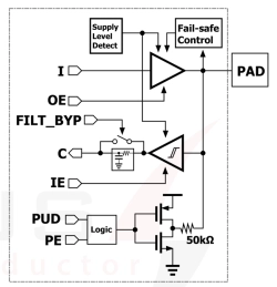
High-voltage solutions in baseline GlobalFoundries and multi-foundry technologies
- High-Voltage ESD
- Physical Features