DDR5 IP for GLOBALFOUNDRIES
Welcome to the ultimate
DDR5 IP
for
GLOBALFOUNDRIES
hub! Explore our vast directory of
DDR5 IP
for
GLOBALFOUNDRIES
All offers in
DDR5 IP
for
GLOBALFOUNDRIES
Filter
Compare
11
DDR5 IP
for
GLOBALFOUNDRIES
from
3
vendors
(1
-
10)
-
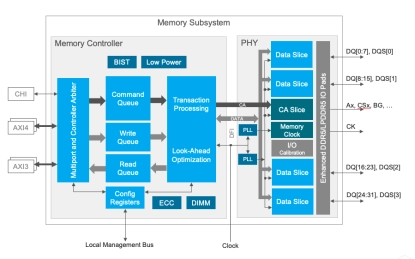
DDR PHY
- DDR5/4/3 training with write-leveling and data-eye training
- Optional clock gating available for low-power control
- Internal and external datapath loop-back modes
- I/O pads with impedance calibration logic and data retention capability
- Programmable per-bit (PVT compensated) deskew on read and write datapaths
- RX and TX equalization for heavily loaded systems
-
DDR5/4 PHY - GF 12LP+
- Supports JEDEC standard DDR5 and DDR4 SDRAMs
- High-performance DDR PHY supporting data rates up to 8400 Mbps
- PHY independent, firmware-based training using an embedded calibration processor
- Supports up to 4 trained states/ frequencies with <3μs switching time

-
DDR multi PHY
- Compatible with JEDEC standard DDR2/DDR3/LPDDR (or Mobile DDR)/ /LPDDR2/LPDDR3 SDRAMs
- Operating range of 100MHz (200Mb/s) to 533MHz(1066Mb/s) in DDR2/DDR3/LPDDR2/LPDDR3 modes
- Operating range of DC to 200MHz in Mobile DDR mode
- PHY Utility Block (PUBL) component
-
DDR4 Multi-modal PHY - GLOBALFOUNDRIES 12nm
- PLL-based clocking with internal clock alignment to the parallel clock on the memory controller interface
- Autonomous initialization
- Support for x72 bit channel
- Support for multiple DRAM widths (x4, x8, x16, x32)
-
DDR4 PHY - GLOBALFOUNDRIES 12nm
- PLL-based clocking with internal clock alignment to the parallel clock on the memory controller interface
- Autonomous initialization
- Support for x72 bit channel
- Support for multiple DRAM widths (x4, x8, x16, x32)
-
LPDDR4X multiPHY Plus in GF (12nm)
- Low latency, small area, low power
- Compatible with JEDEC standard LPDDR4 SDRAMs up to 4,267 Mbps
- Maximum data rate is process technology dependent
- Compatible with JEDEC standard DDR4 SDRAMs up to 3,200 Mbps
-
DDR5/4 PHY in GF (12nm)
- Low latency, small area, low power
- Compatible with JEDEC standard DDR5 SDRAMs up to 8400 Mbps
- Compatible with JEDEC standard DDR4 SDRAMs up to 3200 Mbps
- DFI 5.0 compliant interface to the memory controller
-
LPDDR4 multiPHY V2 in GF (22nm) for Automotive
- Low latency, small area, low power
- Compatible with JEDEC standard LPDDR4 SDRAMs up to 4,267 Mbps
- Maximum data rate is process technology dependent
- Compatible with JEDEC standard DDR4 SDRAMs up to 3,200 Mbps
-
LPDDR4X multiPHY in GF (14nm)
- Low latency, small area, low power
- Compatible with JEDEC standard LPDDR4 SDRAMs up to 4,267 Mbps
- Maximum data rate is process technology dependent
- Compatible with JEDEC standard DDR4 SDRAMs up to 3,200 Mbps
-
DDR3/2 PHY
- ? DDR2/DDR3/DDR3U/DDR3L/LVCMOS operating modes
- ? Compatible with JEDEC standard DDR2/DDR3/DDR3U/DDR3L SDRAMs
- ? Scalable performance from DDR2-667 through DDR3-1600
- ? Maximum controller clock frequency of 400MHz resulting in maximum SDRAM data rate of 1600 Mbps