Arasan Chip System’s xSPI/PSRAM master IP is easy to use, simple to work with, quick to operate, and reliable under all conditions. It supports the xSPI JESD~251 standard from a standard AXI3 or AXI4 slave interface. It also supports HyperRAM, HyperFlash, and features backwards compatibility support for Octal SPI, QSPI, DSPI, and SPI interfaces.
The xSPI/PSRAM master IP is designed so that a user design may immediately access memory from the xSPI device in SPI mode, or alternatively issue a command to switch to any other mode. Additionally, a DMA command may be issued to copy memory to or from the xSPI device and anywhere else on the system bus.
xSPI - PSRAM Master
Overview
Key Features
- SPI Protocol:
- The xSPI Master Core is built around the xSPI protocol, capable of transferring 16-bits on every edge of a 200MHz clock. It remains backwards compatible with the prior Octal SPI, QSPI, Dual SPI and SPI standards.
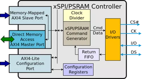
- AXI4 Slave
- The primary interface to this xSPI master IP core is a memory mapped AXI4 slave port. Reads from this port will automatically read from the attached xSPI memory. In the case of either a PSRAM or HyperRAM, writes to this port can also be configured to automatically write to an attached RAM device. AXI WRAP addressing is natively supported in hardware. Further, the xSPI master IP core is optimized for both reads and writes, and therefore capable of maintaining high uninterrupted throughput.
- AXI4 DMA Master
- Finally, this xSPI IP core comes with an internal Direct Memory Access controller with an AXI4 master interface.
- This DMA controller makes it possible to copy data to or from the xSPI interface in a high speed, high throughput, unattended fashion. Using this interface, data may be read from the xSPI master interface and written to the system bus, or alternatively it may be automatically read from the system bus and written to a PSRAM.
- AXI4 – LITE SLAVE
- Moving from one mode or clock speed to another requires interacting with a set of control registers. These control registers allow the xSPI IP to be reconfigured from one mode and clock rate to another. It also allows adjusting any clock-rate dependent parameters of the underlying device interface–required by many QSPI flash devices. Read and write xSPI commands and I/O modes are set from this interface as well, allowing the user to access the device for reading or writing using any command, and any I/O mode.
- The AXI4-Lite slave port also offers access to a raw, low-level device command port. This provides user code with the ability to issue and respond to arbitrary xSPI/PSRAM commands which may be device specific.
- To maintain the xSPI device abstraction, a software library is provided together with the xSPI IP core to both demonstrate how to use this low-level library as well as to document and support user access to these functions.
Block Diagram
Video
Arasan JEDEC compliant xSPI IP a superset of our Octal SPI, QSPI, SPI and PSRAM IP
Arasan Chip Systems, a leading provider of IP for Mobile Storage Standards, presents its JEDEC JESD251C Compliant xSPI IP, a superset of its Octal SPI IP, QSPI IP and PSRAM IP in addition to xSPI providing access to any NOR Flash Device. Arasan's Total xSPI IP, which includes the xSPI PHY IP combines ease of use with high reliability, low power and speed under all conditions, including automotive applications.
Technical Specifications
Maturity
Silicon proven