Processor Architecture for High Performance Video Decode
Processor Architecture for High Performance Video Decode
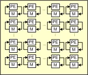
This FFT circuit employs unique architectural characteristics, different than any other FFT implementation.
This FFT circuit employs unique architectural characteristics, different than any other FFT implementation. In particular the locality, simplicity and regularity of the processing core keeps interconnect delays lower than cell delays, leading to clock speeds that can approach the FPGA fabric limitations, e.g., "worst case" Fmax speeds >500MHz in 65nm FPGA technology. Short critical path lengths also lower power dissipation. Additionally, a novel algorithm reduces the number of cycles needed per FFT to less than the transform size. Because the circuit is a "memory based" architecture it is programmable so that a range of transform sizes (even non-powers of 2) can be performed on the same array given adequate memory resources. Finally, it includes a low overhead hybrid floating-point feature that increases dynamic range for a given fixed-point word size.
Note: some files may require an NDA depending on provider policy.

Variable FFT (run time choice of FFT size) is a Filters Transforms IP core from Centar listed on Semi IP Hub.
Engineers should review the overview, key features, supported foundries and nodes, maturity, deliverables, and provider information before shortlisting this Filters Transforms IP.
Yes. Buyers can compare this product with similar semiconductor IP cores or IP families based on category, provider, process options, and structured technical specifications.