NTLab is a vertically integrated microelectronics design center. It has 70+ experienced and qualified engineers.
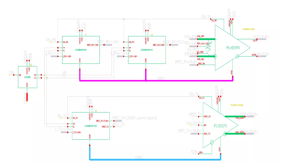
NTLab specializes in the designing of mixed-signal and RF ICs and Systems-on-Chip. It has a wide range of own silicon-verified IP blocks: processor cores, interfaces, analog and high-frequency PHYs, etc., thus allowing customized design to be fast and predictable. In-company unique combination of competences in digital, analog and RF circuits and embedded software enables NTLab to participate in the projects that require deep research and utilize most sophisticated and advanced techniques: multi-system GPS/GLONASS/Galileo/BeiDou/NavIC(IRNSS)/QZSS/SBAS navigation, RF ID, wireless communications, etc. All designed ICs are provided with test and development tools, as well as with reference software.
NTLab offers a wide range of silicon proven analog/mixed-signal IPs in 0.35µm, 0.25 µm, 0.18 µm, 0.13 µm, 0.09 µm, 65nm, 55nm, 40nm, 28nm, 22 nm CMOS and SiGe BiCMOS processes. These IPs are suitable for devices targeted both consumer and industrial markets.
Most of these IPs have been proven in silicon on the foundries: Samsung, UMC, GlobalFoundries, SMIC, VIS, Tower, X-FAB, iHP, AMS, SilTerra, STMicroelectronics, Winfoundry.