Open NAND Flash Interface (ONFI) for NAND Flash Memory chips is an open standard. Arasan’s ONFI 5.0 PHY IP is designed to connect seamlessly with their ONFI 5.0 Host Controller IP. Arasan’s ONFI 5.0 PHY has complete SDR, NV-DDR, NV-DDR2, NV-DDR3 and NV-LPDDR4 TX/RX functionality and supports all the speeds defined in the ONFI specification while remaining backwards compatible with the prior versions of the ONFI specifications. Arasan ONFI 5.0 PHY enables data training, various power drives and ZQ calibration, which ensures maximum operating speed and optimum signal integrity. The PHY uses a PLL / DLL combination to provide very flexible frequency access. The PHY also includes ESD protection on all the various ONFI interface pins. The Arasan’s ONFI 5.0 PHY is an area efficient with a low power consumption and the IO library supports all the features mentioned in the ONFI 5.0 specifications.
ONFI 5.0 PHY
Overview
Key Features
- Designed for seamless integration with Arasan’s ONFI 5.0 Host Controller IP.
- The PHY design supports the newly introduced NV-LPDDR4 mode along with SDR, NV_DDR, and NV_DDR2, NV_DDR3 mode.
- Supports IO voltages at 1.2 V and 1.8 V with core voltage at 0.8V +/-10% and auxiliary power supply at 1.8V +/-10%.
- Includes ONFI 5.0 data I/O PADS and auxiliary I/O PADS with ESD protection structures.
- Includes on-die termination and differential signaling for improved signal integrity at high speeds.
- Integrate PLL and Clock divider to support ONFI 5.0 different mode frequencies.
- Integrate a Master Slave DLL for tuning the Receive clock DQS modes.
- The clock generator {PLL, DLL & CLKDIVIDER} is designed to support different modes of ONFI 4.2 frequencies {20MHz to 860MHz}.
- Built-in diagnostics for monitoring the PLL, DLL and clock divider.
- Includes fractional delay logic in Digital front end of the PHY to correct for skew on both input and output.
- In the Analog Front End (AFE) PHY, CALIO PAD automatically calibrates the source and sink impedance of ONFI I/O and the ODT (On Die Termination) resistors.
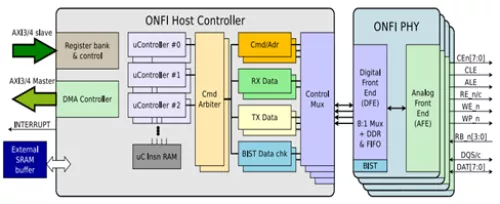
Block Diagram
Technical Specifications
Related IPs
- ONFI 4.0 NAND Flash Controller & PHY
- ONFI 4.1 NAND Flash Controller & PHY & IO Pads on 12nm
- ONFI 4.1 NAND Flash Controller & PHY & IO Pads on 16nm
- ONFI 4.1 NAND Flash Controller & PHY & IO Pads on 28nm
- ONFI 4.1 PHY IP (Silicon Proven in TSMC 12FFC)
- ONFi PHY 4.0 (FPHY+MDLL+SDLL Regulator) (Silicon Proven in TSMC 28HPC+)