The NAND Flash landscape is changing and the Arasan NAND Flash Controller IP Core is changing in accordance with it. New applications are emerging and innovative IP solutions are needed to keep pace. NAND Flash is being incorporated into all types of products including Portable memory drives, Media players, Digital cameras, Smart phones, eBook Readers, Tablets, Digital TVs, Digital camcorders, PCs, and so on. Arasan is in the perfect position to give you what you need.
The Arasan NAND Flash Controller IP Core is a full featured, easy to use, synthesizable core, easily integrated into any SoC or FPGA development. Designed to support SLC, MLC and TLC flash memories, it is flexible in use and easy in implementation. The controller works with any suitable NAND Flash memory device up to 1024Gb from leading memory providers – Micron, Samsung, Toshiba and Hynix. The IP core includes a host of configuration options from page size to bank selects. The controller offers Hamming Code (1-Bit error correction and 2-Bit error detection) and BCH (option for 4-, 8-, 12-, up to 32-Bit error correction) Error Code Correction (ECC) for optimized performance and reliability. Additional features include the capability to boot from flash.
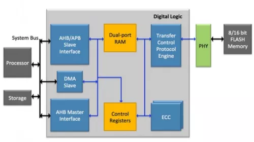
The IP core supports the Open NAND Flash Interface Working Group (ONFI) 3.2, 4.0 and 4.1 standards. It can also support a variety of host bus interfaces for easy adoption into any design architecture – AHB, APB, OCP, 8051 or custom buses. The slave AHB IP supports an external DMA interface where the master AHB incorporates an internal DMA controller.
The Arasan NAND Flash Controller IP Cores are delivered in Verilog RTL that can be implemented in an ASIC or FPGA. They are fully tested with vendor models and hardware is tested with FPGA’s. The core includes RTL code, test scripts and a test environment for complete simulation and verification.
NAND Flash Interface
The NAND Flash Interface handles all the command, address and data sequences and manages all the hardware protocols. It is ONFI 3.2, 4.0 and 4.1 compliant and provides an 8-bit or 16-bit interface to the flash memories. The interface supports a maximum of 1024 Gb of NAND flash memory. All timing modes (0-5) are supported for SDR, NV-DDR and Timing modes (0-10) for NV-DDR2 and Timing mode (0 – 12) for NV-DDR3.
AHB Slave Interface
The AHB Slave block consists of the operational registers. A processor connecting to the custom interface can control the operation of the NAND Flash controller through the NAND Flash control registers. Read/write operations of the flash memory can be performed through NAND flash interface.
AHB Master Interface
NAND Flash controller acts as a master during MDMA mode of transaction. The AHB master interface places control signals in AHB Bus depending upon the FIFO status. During Write transaction, AHB master interface reads data from system memory and stores into the FIFO. During Read transaction, reads data from FIFO and stores into system memory. AHB master interface asserts DMA interrupt when DMA buffer boundary is reached. The AHB master interface can be used to transfer boot code from the NAND flash memory to the system memory during system power-up.
Two Port RAM (1R1W)
This block has handshake logic to communicate with the AHB interface and on the other side communicates with the Flash Interface. Typical RAM size is 256×32 (or 128×64), to support block size of 512 bytes. The FIFO depth is configurable.
ECC
The ECC module provides error detection and correction support for SLC Flash memory as well as the MLC and TLC Flash memory. For SLC Flash, Hamming Code is being used for 1 bit error correction and 2 bit error detection. BCH Code, capable of up to 32-Bit error correction, is used for MLC and TLC Flash devices. An optional pipeline stage in the BCH decoder can be enabled for maximum performance.
Control Registers
The host processor controls the configuration and operation of the NAND Flash Controller through the Control Registers. Configuration includes the set up time (tCCS, tDQSQ, tDS), memory configuration (address, page size, packet size, packet count), timing modes (SDR, NV-DDR, NV-DDR2 and NV-DDR3), and so on. The Control Registers also provide operating status such as Busy and Data Ready signals.
Slave DMA Interface (Optional)
This interface is used to perform a SDMA mode of Write/ Read data transfer. Slave DMA Interface provides DMA Request, DMA Single and DMA Last and gets acknowledged by DMA Acknowledge and DMA Finish. DMA Request is asserted until the required amount of data is transferred based on the DMA Transfer count. For the generated DMA Request Slave DMA Controller provides write data for write transfer or reads the data from FIFO for read transfer.
ONFI 4.1 NAND Flash Controller & PHY & IO Pads on 12nm
Overview
Key Features
- ONFI 4.1 NAND Flash Controller
- Flash devices up to 1024Gb
- NAND Flash memories from Micron, Samsung, Toshiba and Hynix
- Boot mode support
- LUN Set/ LUN Get feature support
- All mandatory commands and selected optional commands
- Full access to spare area
- Speed ranging from 40MB/s to 1200MT/s to allow applications to balance performance and power
- Multi LUN/DIE Operations
- Small Data Move
- Change Row Address
- Reset LUN
- EZ – NAND devices
- Chip_en pin reduction mechanism
- ODT Configure
- On-die termination
- Supports Interleaving Operations:
- Page Program Interleaving
- Copy back Program Interleaving
- Block Erase Interleaving
- Read Interleaving
- Cache Interleaving
- ONFI 4.1 PHY
- Compliant to ONFI specification version 4.1
- Supports NV-DDR3 mode of operation supporting up to 600MHz
- Supports NV-DDR2 mode of operation supporting up to 400MHz
- Supports NV-DDR mode of operation supporting up to 100MHz
- Supports legacy Asynchronous devices operating from 10MHz to 50MHz
- Can be used with Arasan’s ONFI 4.1 NAND Flash Controller IP
- Supports 1.2V & 1.8V operation I/O pads
- Dynamically center aligns the DQS for better noise margin and immune to PVT variations with the use of analog DLL
- Supports up to +/-200ps of bit level deskew on READ and WRITE
- Supports differential signaling of DQS and RE signals
- Supports four levels of drive strength as mentioned in the ONFI 4.1 standard
- Supports Manufacturability tests – DC SCAN and ABIST
Benefits
- Page Size – 2KB, 4KB, 8KB, 16KB
- Bank/chip select options
- Programmable timing
- Address cycles – 4, 5
- ECC enable, disable
- RAM size – 1KB, 2KB and 4KB
- Supports parallel connection of two 8-bit flash devices
Block Diagram
Deliverables
- ONFI 4.1 Controller
- RMM Compliant Synthesizable RTL design in Verilog
- Easy-to-use test environment
- Synthesis scripts
- Technical documents
- ONFI 4.1 PHY
- GDS-II Database
- LVS Netlist
- Physical Abstract Models (LEF)
- Timing Models (LIB)
- Process Specific Integration Guide
Technical Specifications
Maturity
Silicon Proven
Availability
Now
TSMC
Silicon Proven:
12nm