The NAND Flash landscape is changing and the Arasan NAND Flash Controller IP is changing with it. New applications are emerging and innovative IP solutions are needed to keep pace. NAND Flash is being incorporated into all types of products including portable memory drives, media players, digital cameras, Smart Phones, eBook Readers, Tablets, digital TVs, digital camcorders, PCs, etc. Arasan is in the perfect position to give you what you need.
The Arasan ONFI 4.0 NAND Flash Controller IP is a full featured, easy to use, synthesizable core, easily integrated into any SoC or FPGA development. Designed to support SLC, MLC and TLC flash memories, ONFI 4.0 NAND controller IP is flexible in use and easy in implementation. The controller works with any suitable NAND Flash memory device up to 1024 Gb from leading memory providers. The IP includes a host of configuration options from page size to band selects. The controller offers Hamming Code (1-Bit error correction and 2-Bit error detection) and BCH (option for 4-, 8-, 12-, up to 32-Bit error correction) error correction code (ECC) for optimized performance and reliability. Additional features include the capability to boot from flash.
This NAND Controller IP supports the ONFI 4.0 and earlier standards and the Micron ClearNAND. It can also support a variety of host bus interfaces for easy adoption into any design architecture – AHB, APB, OCP, 8051 or custom buses. The slave AHB IP supports an external DMA interface where the master AHB incorporates an internal DMA controller.
NAND Flash Interface
The NAND Flash Interface handles all the command, address, and data sequences and manages all the hardware protocols. It is ONFI 4.0 compliant and provides an 8-bit or 16-bit interface to the flash memories. The interface supports a maximum of 1024 Gb of NAND flash memory. SDR, NV-DDR, NV-DDR2 and NV-DDR3 data interfaces are supported. Timing modes (0-5) are supported for SDR, NV-DDR and Timing modes (0-10) are supported for NV-DDR2, NV-DDR3.
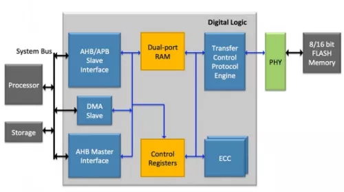
AHB/APB Interface
The AHB/APB master/slave block consists of the operational registers. A processor connecting to the system bus can control the operation of the NAND Flash controller through the NAND Flash control registers. Read/write operations of the flash memory can be performed through the DPRAM or NAND flash interface. The AHB/APB master interface can be used to transfer boot code from the NAND flash memory to the system memory during system power-up.
Host Interface
Arasan supports many system buses including AHB, APB, OCP, and custom buses. A host connecting to the system bus controls the operation of the ONFI NAND Flash Controller through the NAND Flash Control Registers. Read/write operations of the flash memory can be performed through the DPRAM or NAND flash interface.
Control Registers
The host processor controls the configuration and operation of the ONFI NAND Flash Controller through the Control Registers. Configuration includes the setting of hold time, setup time, wait state, memory configuration, timing modes, etc. The Control Registers also provide operating status such as Busy and Data Ready signals.
Software Stack and NAND Flash File system
A software stack and a NAND Flash file system are available as an option to the ONFI NAND Flash Controller IP. Designed specifically to work with Arasan ONFI NAND Flash IP, they are optimized to support key features of the IP core. Designed for Linux operating system, they can be easily ported to a variety of other operating systems to fit any application.
ECC
The ECC module provides error detection and correction support for SLC, MLC and TLC Flash memory. Hamming based block codes are the most commonly used ECC for SLC devices and BCH which is able to handle multiple errors and are widely used on MLC and TLC flash devices. For more protection of data we can use optional BCH code in SLC flash devices. An optional pipeline stage in the BCH decoder can be enabled for maximum performance. An optional configuration to select the data block size and the number of bit errors to be corrected is available.
ONFI 4.0 PHY &I/O PADS
• Silicon proven PLL to support all frequencies from 10MHz to 400MHZ, and DLL to improve
data sampling accuracy dynamically
• Includes I/O pads compatible to 1.2v NV-DDR3 800MT/s, 1.8v NV-DDR2 800MT/s and 3.3v or
1.8v NV-DDR 200 MT/s
• Supports NV-DDR3 mode of operation supporting up to 400MHz
• Supports NV-DDR2 mode of operation supporting up to 400MHz
• Supports legacy Asynchronous devices operating from 10MHz to 100MHz
• Supports differential signaling of DQS and RE signals
ONFI 4.0 NAND Flash Controller & PHY
Overview
Key Features
- • Support ONFI 4.0, EZ – NAND, Standard ClearNAND, Advanced ClearNAND
- • Support standard asynchronous NAND flash
- • High performance from 40MT/s to 800MT/s
- • High density NAND flash up to 1024 Gb
- • EZ-NAND devices
- • Chip_en pin reduction
- • On-Die-Termination Configure
- • Supports 5 Interleaving Operations
- Page, Copy back, Block Erase, Read, Cache
- • Supports Multi LUN/DIE Operations
- • Supports Small Data Move
- • Supports Change Row Address
- • Supports Reset LUN
- Micron ClearNAND Features
- • CE# pin reduction
- • Volume addressing and select command
- • Interrupt signals command completion
- • Volume Select, LUN Status, Device Status, Operation status, Get Next Operation Status
Benefits
- ONFI 4.0 Interface supports up to 1TB of storage
- NVDDR3 supports up to 1.6GB/s bandwidth
Block Diagram
Deliverables
- ONFI 4.0 Controller
- RMM Compliant Synthesizable RTL design in Verilog
- Easy-to-use test environment
- Synthesis scripts
- Technical documents
- ONFI 4.0 PHY
- GDS-II Database
- LVS Netlist
- Physical Abstract Models (LEF)
- Timing Models (LIB)
- Process Specific Integration Guide
Technical Specifications
Maturity
Silicon Proven
Availability
Now