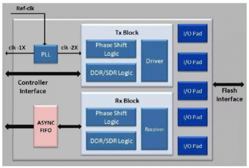
Compliant to ONFI 3.2 electrical interface, the ONFI 3.2 PHY, delivered in hard macro, is process technology proven and easy to integrate. This ONFI 3.2 PHY, supporting NV-DDR2 up to 400MT/s with capability of scaling speed, accelerates time-to-market by reducing SoC designers’ development time otherwise spent on ensuring high speed signal integrity
ONFI 3.2 NV-DDR2 PHY in GDSII
Overview
Key Features
- Compliant to ONFI revision 3.2 standard
- Supports NV-DDR2 mode of operation supporting up to 266MHz or 566MT/s
- Supports NV-DDR mode of operation supporting up to 100MHz
- Supports legacy Asynchronous devices operating from 10MHz to 50MHz
- Can be used with any other ONFI digital controller
- Includes 1.8V/3.3V operation I/O pads complaint to ONFI 3.2, ONFI 3.1, ONFI 2.3, ONFI 2.0
- Contains a PLL to support all frequencies from 10MHz to 200MHz
- Uses 2X clock for better timing
- Contains a DLL to align the DQS for better noise margin and immune to PVT variations
- Supports differential signaling of DQS and RE signals
- Supports 4 levels of drive strength as mentioned in the ONFI 3.2 Standard
Benefits
- Proven and robust high performance ONFI 3.2 NV-DDR2 PHY delivered in hard marco
- Offered as a Total IP solution including RTL Host Controller IP, Verification IP and ESL models, Software Stack, and Hardware Development Platform
- Arasan Chip Systems is the leading supplier of mobile storage IP and its products are used by most first tier memory suppliers. Extensive experience and compliance testing with all versions of this specification make the choice of Arasan products the lowest risk approach to implementation of ONFI NAND flash enabled products.
- Arasan’s development engineering team provides direct support to customers insuring that the highest level of knowledge is immediately available to the customer thus reducing problem resolution time.
Block Diagram

Deliverables
- The full IP package complete with:
- Graphic Design System II (GDSII) database
- Layout Versus Schematic (LVS) Netlist
- Physical Abstract Model (LEF)
- Behavioral Models
- Design Integration Guide
- Technical Documentation
Technical Specifications
Maturity
contact sales
Availability
contact sales