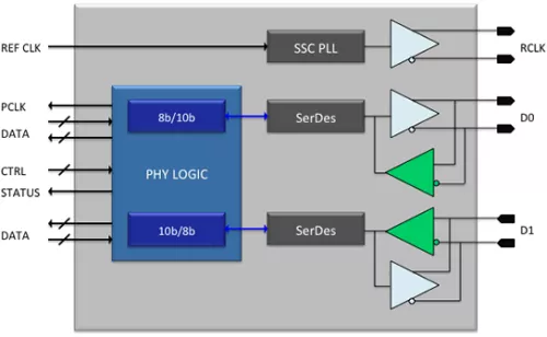
SD 4.0 (UHS-II) achieves a peak interface speed of 3.12 Gbps. Arasan’s UHS-II PHY is compliant with the specification of UHS-II and is an extremely area and power efficient implementation. This interface is backward compatible with legacy SD cards. Both Host and Device UHS-II PHY configurations are available from Arasan.
The UHS-II PHY IP is a comprehensive, silicon-proven configurable core that has been ported to multiple process nodes and leading foundries. It uses sub-LVDS signaling consisting of one pair each for transmit, receive and an additional reference clock. This low-pin count interface has reduced power consumption and low Electro Magnetic Interface (EMI). To further reduce power, the reference clock operates at 1/15th or 1/30th of the data transfer speed. This differential clock operates between 26MHz to 52 MHz and is carried over the legacy SD lines DAT0, and DAT1.
Arasan’s UHS-II PHY operates in both the Full-duplex and Half-duplex modes. It includes an 8b/10b encoder/decoder. The controller side of the interface of the UHS-II
PHY operates in the range between 39 Mbps to 156 Mbps. The default data lane D0 is used for downstream connection and the D1 lane is used for the other direction. An 8b/10b coding scheme is used. To improve testability, the UHS-II PHY implements the standard loopback paths.
SD 4.0 UHS-II PHY in TSMC 40LP
Overview
Key Features
- Compliant to SD Specifications Part 1 UHS-II Specification Volume 2: PHY* and SD Specifications Part 1 UHS II
- Specification Volume 1: System and Protocol”
- Per lane data rate between 390Mb/s to 1.56Gb/s
- Supports peak interface speed of 3.12Gb/s (Half-duplex); 1.56Gb/s in Full-duplex mode
- Sub-LVDS Differential PHY signaling
- Low frequency differential reference clock (1/15 or 1/30) of data rate Supports Spread Spectrum clocking to reduce EMI
- Flexible transmission rates from 390Mb/s – 1.56Gb/s (each lane) Multiple power saving modes: Dormant, Line standby
- Low power, reduced EMI operation
- Integrated solution with built-in termination, no external components required
- Easily ported to various process nodes and foundries
Benefits
- Silicon proven, fully compliant core
- Premier direct support from Arasan IP core designers
- Easy-to-use industry standard test environment
- Unencrypted source code allows easy implementation
- Reuse Methodology Manual guidelines (RMM) compliant verilog code.
Block Diagram

Deliverables
- GDSII database
- LVS Netlist
- Physical Abstract Model (LEF)
- Timing Models
- Behavioral Models
- Design Integration Guide
- Technical Documentation
Technical Specifications
Maturity
Silicon Proven
Availability
Now