MIPI D-PHY V1.2@2.5GHz TSMC28nm HPC+

Overview

The MIPI D-PHY analog IP is available in foundry processes spanning 28nm to 180nm. 
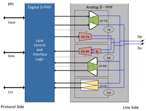
The bidirectional MIPI D-PHY Analog Transceiver IP Core is fully compliant to the D-PHY specification version 1.1. It supports the MIPI® Camera Serial Interface (CSI-2) and Display Serial Interface (DSI) protocols. It is a Universal PHY that can be configured as a transmitter, receiver or transceiver. The D-PHY consists of an analog front end to generate and receive the electrical level signals, and a digital back end to control the I/O functions.

The D-PHY provides a point to point connection between master and slave or host and device that comply with a relevant MIPI® standard. A typical configuration consists of a clock lane and 1-4 data lanes. The master/host is primarily the source of data and the slave/device is usually the sink of data. The D-PHY lanes can be configured for unidirectional or bidirectional lane operation, originating at the master and terminating at the slave. It can be configured to operate as a master or as a slave. The D-PHY link supports a high speed (HS) mode for fast data traffic and a low power (LP) mode for control transactions. In HS mode, the low swing differential signal is able to support data transfers from 80 Mbps to 1.5 Gbps. In LP mode all wires operate as a single ended line capable of supporting 10 Mbps asynchronous data communications.

The D-PHY Analog Transceiver IP core implements the PPI interface recommended by the MIPI® working groups to easily interface to the required protocols.

Key Features

  • Compliant to MIPI Alliance Standard for D-PHY specification Version 1.1
  • Supports standard PHY transceiver compliant to MIPI Specification
  • Supports standard PPI interface compliant to MIPI Specification
  • Supports synchronous transfer at high speed mode with a bit rate of 80-2500 Mb/s
  • Supports asynchronous transfer at low power mode with a bit rate of 10 Mb/s
  • Spaced one hot encoding for Low power [LP] data
  • Supports ultra low power mode, high speed mode and escape mode
  • Supports one clock lane and up to four data lanes
  • Data lanes support transfer of data in high speed mode
  • Clock lane supports unidirectional communication
  • Supports High speed mode in Forward communication
  • PHY can be configured as a master or slave
  • One byte buffer is housed inside the core for both data-out and data-in paths
  • Activates and disconnects high speed terminators for reception and transmission
  • Supports error detection mechanism for sequence errors and contentions
  • Supports contention detection and turn-arounds
  • Testability for Tx, Rx and PLL
  • Has clock divider unit to generate clock for parallel data reception and transmission from/to the PPI unit
  • On-chip clock generation configurable for either transmitter or a receiver
  • Process & Foundry
  • Available in various foundry processes
  • No external (off-chip) components required
  • Can be ported to other processes

Benefits

  • Available in various foundry processes
  • No external (off-chip) components required
  • Can be ported to other processes.
  • Silicon proven
  • Extensive Quality Methodology

Block Diagram

MIPI D-PHY V1.2@2.5GHz TSMC28nm HPC+ Block Diagram

Deliverables

  • GDS-II Database
  • LVS Netlist
  • Physical Abstract Models (LEF)
  • Timing Models (LIB)
  • Process Specific Integration Guide

Technical Specifications

Maturity
Silicon Proven
Availability
Now
×
Semiconductor IP