MIPI D-PHY Universal IP in Samsung 28FDSOI
Overview
Key Features
- Supports MIPI® Specification for D-PHY Version 2.1.
- Consists of 1 Clock lane and up to 4 Data lanes.
- Supports both high speed and low-power modes.
- 80 Mbps to 1.5 Gbps data rate per lane without Deskew calibration.
- Up to 2.5 Gbps data rate per lane with Deskew calibration.
- 10 Mbps data rate in low-power mode.
- Low power dissipation.
- Loopback testability support.
- Optional resistance termination calibrator.
- Deskew calibration support.
Benefits
- Low power
- Small area
- Universal configuration supports CSI-2 and DSI
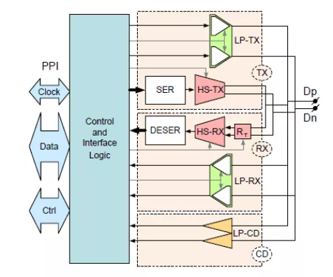
Block Diagram

Video
Lattice Crosslink-NX featuring Mixel's MIPI D-PHY IP
In this Mixel customer demo video, we see Mixel’s MIPI D-PHY IP integrated into the Lattice CrossLink-NX FPGA, the world’s first low-power FPGA to support D-PHY v1.2 with 2.5Gbps per lane and the previous generation FPGA, Lattice Crosslink which was the first bridge supporting 12 Gbps of Aggregate Bandwidth. Built using the new 28 nm FD-SOI Lattice Nexus™ FPGA platform, the CrossLink-NX FPGAs outperform FPGAs of similar class in terms of power, form factor, reliability, and performance. The CrossLink-NX FPGAs were developed for use in applications including sensor and display bridging, sensor aggregation, sensor duplication, and AI inferencing at the Edge. The previous generation Lattice CrossLink bridge combines the flexibility and fast time to market of an FPGA with the power and functional optimization of an ASSP to create a new product class called programmable ASSP (pASSP™). This solution, which is now going into production, integrates Mixel’s high performance, low power Universal MIPI D-PHY, implemented in UMC’s 40nm process to achieve first silicon success.
Applications
- Mobile
- Displays
- Cameras/Sensors
- IoT
- VR/AR/MR
- Consumer electronics
- Automotive
Deliverables
- Specifications
- GDSII
- LVS netlist
- LEF file
- IBIS Model
- Verilog Model
- Timing Model
- Integration Guidelines
- RTL
- Documentation
- One year support
Technical Specifications
Related IPs
- MIPI D-PHY Verification IP
- MIPI D-PHY DSI TX (Transmitter) in Samsung 28FDSOI
- MIPI D-PHY CSI-2 RX (Receiver) in Samsung 28FDSOI
- MIPI D-PHY/LVDS Combo TX (Transmitter) for Automotive in Samsung 28FDSOI
- Ultra Low Power Embedded SRAM - Samsung 28FDSOI
- Neural engine IP - The Cutting Edge in On-Device AI