2.8 Gbps LVDS IO
Overview
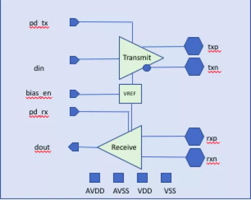
The LVDS I/O is a single macro (input, output and reference block). Both driver and receiver operating up to 1.4GHz (2.8 Gbps ). The Driver is designed to drive 100? differential termination.
Key Features
- Powered from 1.8V ±5% and 0.9V(±10%) core power supplies
- Operates up to 1.4GHz (2.8Gbps)
- Powered from 1.8V ±5% and 0.9V (±10%) core power supplies
- PADS include ESD structures
Benefits
- Different bump options for optimum usage of I/O ring
- Power down feature for saving power
Block Diagram

Applications
- Chip to Chip interface on a PCB or similar applications
Deliverables
- Abstract - LEF
- Behavioral model - Verilog
- Timing model - .LIB
- LVS model - CDL
- Physical - .GDS2
Technical Specifications
Foundry, Node
TSMC 28nm HPC, HPC+
Maturity
GDS2 ready
Availability
Immediate
Related IPs
- 1.25 Gbps Four-Channel (4CH) LVDS Serializer with Pre-emphasis
- IO & ESD solutions supporting GPIO, I2C,RGMII, SD, LVDS, HDMI & analog/RF across multiple technology nodes
- 1.6 Gbps DDR Programmable LVDS Transmitter/Receiver
- 1 Gbps DDR LVDS transmitter
- 1 Gbps DDR rail to rail LVDS receiver
- 2.4 Gbps LVDS transmitter