Usage of Multibit Flip-Flop and its Challenges in ASIC Physical Design
Sarvang Sanghavi, Ravish Shah, Upendra Somashekaraiah (eInfochips)
Abstract:
The continuous need for reduced size of the chip in the VLSI industry brings exciting challenges to the layout engineers for designing better and high-performing integrated circuits, which needs to consume low power even while reducing the silicon area and cost involved. Internal power is a component of the total power consumed by the chip, which is becoming more challenging to handle with the shrinking technology nodes. There are many methods, which have been used to reduce the internal power in the industry. In this article, we will discuss the usage of multibit flops in the design to reduce the power component of the ICs. We will also discuss other design challenges faced while using the multibit flip-flops (MBFF) and ways to overcome them.
Introduction to multibit flop:
Multibit flops are used to reduce the power in ASIC without affecting the performance of the design. Multibit flops as the name suggests have multiple D and Q pins. Generally, two bit and four bit versions are available in the library. A two bit multibit flops will have D0, D1, Q0, Q1 pins along with a common clock, scan_in and scan_enable pins. In a two bit flop, the scan_in pin of the second bit flop is connected to the first flop Q pin (Q0), so that they are in scanning order. The layout of the multibit flop is designed in a compact manner so that the effective area of the multibit flop is much lesser than the added area of the single bit flops (Fig2, Fig3, and Fig4). For example, two bit multibit flop has roughly 20% lesser area than the combined area of the two single bit flops of the same drive strength. A two bit flip-flop can be designed to have a single cell row height or two cell row height (single cell row two bit flop is shown in Fig3), while a four bit flop is designed with two rows height (Fig4).
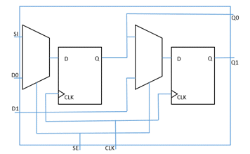
Fig1: Simplified representation of two bit flip-flop

Fig2: A single bit flop layout view

Fig3: Two bit flop layout view

Fig4: Four bit flop layout view
Clock pin of the multibit flop drives more load compared to the clock pin of the single bit flop. Hence, a more robust clock driver is used internally while designing the multibit flip-flop. However, the library setup and hold time (which depends on the clock and data transition), as well as the clock-to-Q delay (which depends on clock transition and load at the Q pin) will be more than the normal flop. Clock to Q delay for the Q0 and Q1 pin of the two bit flip-flop will have a variation of 2 - 8% between them. Clock to Q delay for Q0 pin will be higher than Q1 pin as the Q0 pin sees an additional load of connection for scan_in mux pin for the second level.
Example Cases:
Multiple experiments were conducted while doing physical design implementation for sub blocks with both multibit flops and without multibit flops. The observations from these experiments have been captured below.
Reduction of clock power using the multibit flops:
Input capacitance at the clock pin of the multibit flip-flop will not vary much compared to the single bit flop; we can observe a difference of about 5% in the values. This effect will significantly reduce the clock switching power component of the design as the clock tree cell driving the leaf pins will see a much lesser load. Leakage power of the multibit flop also shows a greater advantage over the normal bit flops, providing a 20% improvement.
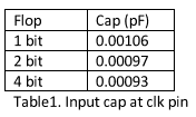
From the above table, if we use 4 single bit flops, the total input pin capacitance would be 0.00424 pF whereas, with a 4-bit flop, it would be only 0.00093 pF. This will help a single buffer to drive more number of flops and hence, we can also see a reduction in the number of clock tree buffers. Also, low drive strength buffers can be used to build the cock tree which will save power. We can observe a 25-30% reduction in the clock-tree buffer count with the usage of multibit flops.
With regards to the advantage we have with pin capacitance of multibit flop as compared to single-bit, it should be noted that less clock buffers would be used for building the clock tree in the case of multibit flops. Below table shows the buffer usage and the drive strength. It is evident from the below table that CTS (clock tree synthesis) in single-bit flops uses more number of buffers and high drive (adding X12, X16) strength buffers. This helps in reducing the dynamic power of the design.
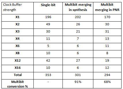
Table 2: Number of clock buffers used in the single bit and multibit experiment
The disadvantage of enabling multibit merging at the synthesis stage is that the tool will automatically performs the merging when the flops belong to the same hierarchy. This poses a serious limitation on how the hierarchy placement is being done. That is why we see a few buffers while merging at the placement stage. It can be done based on the floorplan shape and also the timing requirement of the flops. (See more in the Implementation section).
Better clock tree and routability:
In Fig5 and Fig6, we can see how a clock tree is built from the same clock gating cell in different experiments, with and without multibit flops. In case of non-multibit flops experiments, a clock tree of multiple levels of buffers is built from ICG (Integrated Clock Gating) to supply the clock to flops. In case of multibit flops experiments, the buffers are less. This improves the routability and will help in the convergence of routing.

Fig5: Clock tree without multibit flops

Fig6: Clock tree with multibit flops
Implementation:
To use multibit flops in the design, we will have to convert the existing single bit flops to multibit flops. This can be done at the synthesis stage or at the placement stage.
Synthesis in WLM (Wire Load Model) or PLE (Physical Layout Estimation) mode will have a relaxed setup timing and will not take into account the floorplan shape. Hence, the multibit merging ratio would be very high in this case, but we may see some timing surprises during PnR (Place and Route). We generally see up to 90% multibit conversion in synthesis.
Multibit conversion in PnR is timing-aware. It takes care of the floorplan shape, macro placement, hierarchy placement, and placement of flops. With this, we see around 65% of conversion rate. This is low compared to multibit conversion at synthesis, but gives better QoR (Quality of Results)
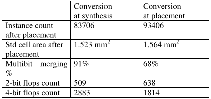
Table 3: Comparison of multibit conversion at synthesis and placement stage
Challenges and Solutions:
Performing timing ECO (Engineering Change Order):
Multibit flops have a common clock pin and test pins. Performing ECO on these pins would be difficult if we are targeting only one bit out of 2 or 4 bits. For example, if we want to adjust the clock skew at the ECO stage to recover any timing violations for a particular bit, the additional skew adjusted will affect other bits of multibit flop. If this is affecting the timing of other bits of the flops, we may need to break this multibit flop into single bit flops and do eco connections and routing. If the ECO is metal only then it would be more difficult to find spare flops and perform ECO.
Increased pin density:
One drawback of having multibit in the design is the high pin density. Pin density should not be confused with the number of pins. Though MBIT has less pins (almost half) compared to the single bit, the local pin density in a bin is particularly high. Moreover, MBITs will have more pin routing blockages and pin metal layers. Below are the pin shape figures for a single bit and 2 bit flops.
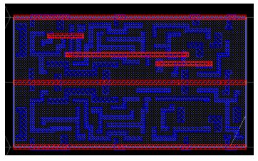
Fig 7: Multibit Pin Shapes
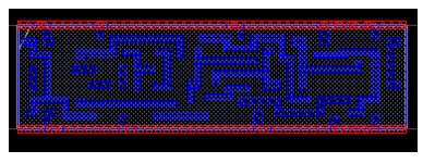
Fig 8: Single flop pin shapes
As it is seen from the above images, multibit is also using Metal 2 (red color layer) as an obstruction layer, whereas, a single bit is only using Metal 1 as an obstruction layer.
Below is the pin density report of the design with and without multibit. Here, we have divided the entire design in rectangular bins of 8.61x8.61 microns. Below table indicates the number of bins having a high pin density.
Bin size used for capturing the pin density = 8.610 by 8.610 Microns
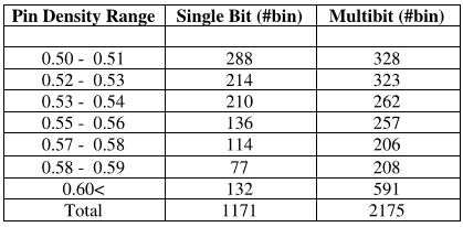
Table 4: Pin density comparison
Multibit experiment: Number of bins with pin density more than 0.5 = 3.78 % Singe bit experiment: Number of bins with pin density more than 0.5 = 2.04 %
Taking care of the high pin density: High pin density may result in high localized congestion over the multibit flops. There are different ways to avoid such issues,
- Cell padding
- Instance Padding
- Avoid placing multibit below power straps.
IR/EM issue with MBIT:
When the clock pin of the Multibit toggles, both the flops and their internal clock circuitry will draw current even though only one of them is changing the state. This can lead to high current getting drawn from the power rails. This requires a robust power network and an addition of Decoupling capacitors around the multibit flops. This also means that the short-circuit current requirement of multibit flops would be higher than a single bit flop in a localized region.
One way to avoid IR/EM issue is to reserve space around the multibit flop by applying cell padding and removing the pad during de-caps insertion.
Conformal checks:
During RTL to synthesized netlist conformal checks, we need to instruct the tool to split the multibit flops into a single bit and do the verification. When the multibit conversion happens, the tools follow a particular naming convention with prefix and separator to identify the multibit flops. With these naming conventions, the multibit flops can be broken down into single bit flops during the conformal checks.
Conclusion:
Multibit flops offer a smart way to reduce the overall power of the design without impacting the timing. Usage of multibit flops reduces the leakage power and the dynamic power by reducing the clock tree cells and holding the buffers required in the design. It also helps in improving the density of the design by reducing the standard cell area, and thereby optimizing the block size.
Authors:
Upendra Somashekaraiah works as a Technical Manager at eInfochips, an Arrow company. He has more than 12 years of experience in ASIC Physical Design.
Ravish Shah works as a Senior Engineer at eInfochips, an Arrow company. He has more than three years of experience in ASIC Physical Design.)
Sarvang Sanghavi is an Engineer at eInfochips, an Arrow company Pvt Ltd. He has over two years of experience in the ASIC Physical Design.)
About eInfochips:
eInfochips, an Arrow company, is a leading global provider of product engineering and semiconductor design services. With over 500+ products developed and 40M deployments in 140 countries, eInfochips continues to fuel technological innovations in multiple verticals. The company’s service offerings include digital transformation and connected IoT solutions across various cloud platforms, including AWS and Azure.
Along with Arrow’s $27B in revenues, 19,000 employees, and 345 locations serving over 80 countries, eInfochips is primed to accelerate connected products innovation for 150,000+ global clients. eInfochips acts as a catalyst to Arrow’s Sensor-to-Sunset initiative and offers complete edge-to-cloud capabilities for its clients through Arrow Connect.
Related Semiconductor IP
- ReRAM NVM in DB HiTek 130nm BCD
- UFS 5.0 Host Controller IP
- PDM Receiver/PDM-to-PCM Converter
- Voltage and Temperature Sensor with integrated ADC - GlobalFoundries® 22FDX®
- 8MHz / 40MHz Pierce Oscillator - X-FAB XT018-0.18µm
Related Articles
- Bigger Chips, More IPs, and Mounting Challenges in Addressing the Growing Complexity of SoC Design
- AI in VLSI Physical Design: Opportunities and Challenges
- Integrating VESA DSC and MIPI DSI in a System-on-Chip (SoC): Addressing Design Challenges and Leveraging Arasan IP Portfolio
- Role of Embedded Systems and its future in Industrial Automation
Latest Articles
- An FPGA-Based SoC Architecture with a RISC-V Controller for Energy-Efficient Temporal-Coding Spiking Neural Networks
- Enabling RISC-V Vector Code Generation in MLIR through Custom xDSL Lowerings
- A Scalable Open-Source QEC System with Sub-Microsecond Decoding-Feedback Latency
- SNAP-V: A RISC-V SoC with Configurable Neuromorphic Acceleration for Small-Scale Spiking Neural Networks
- An FPGA Implementation of Displacement Vector Search for Intra Pattern Copy in JPEG XS