Understanding Physical Unclonable Function (PUF)
Why Physical Unclonable Functions (PUF)?
20 years ago, digital security was implemented only in dedicated electronic devices such as banking cards or payment terminals. Today everyone connects to its bank using a secure internet connection signaled by "https://" and we all expect that the information we manipulate with our smartphone is protected. Cryptographic techniques such as encryption or digital signature have been deployed to meet these requirements. As a consequence, a growing number of ASICs, microcontrollers and SoCs embed hardware cryptographic accelerators or software cryptographic libraries. The emergence of the Internet of Things (IoT) will call for an even faster adoption. We now can talk about cryptography pervasion.
Such pervasion has been made possible because in modern cryptography algorithms are public and standardized. The immediate consequence of algorithms being publically known is that keys become the most valuable assets, hence they must be strongly protected.
Historically, the first Integrated Circuits (IC) designed to strongly protect keys were the smartcard ones. With the growing need for digital security, cryptography has been implemented in more and more ICs such as generic microcontrollers but the protection of keys is always a challenge. We can see today several options:
- No specific protection implemented. This should never happen but unfortunately it still does!
- In circuit logical protection such as TrustZone™. The keys are protected against logical attacks such as malwares but not against physical attacks.
- In circuit logical and physical protection.
- Key storage in an separate dedicated IC, external to the main processor, called a "Secure Element"
The choice of a key protection scheme in an Integrated Circuit (IC) depends on many factors:
- Availability of an adequate IC manufacturing technology: the presence of Non Volatile Memory such as EEPROM or Flash influences directly the way keys can be physically protected
- Market requirements: the level of security implemented in an IC depends on its end usage.
- IC Designer know-how: designing hardware protection blocks is still a matter of experts
- Time to market
- Development cost
- Cost per unit (additional die area)
One may think that physical protection is not necessary in most cases. This is no longer true since automated reverse engineering associated with failure analysis techniques has made physical attacks affordable [1].
The traditional way of designing secure key storage consists in storing the keys in a non-volatile memory (OTP, EEPROM or Flash) and implement layout countermeasures or obfuscation such as die shield, bus scrambling or dummy vias [2]. A more robust solution relies on memory encryption through a master key, but then the challenge is the protection of the master key itself and we are back to the initial challenge.
This approach is valid and is proven by certifications such as Common Criteria. Typically, an EAL4+ certification or above includes the component "AVA_VAN.5" which rates the resistance of an IC against physical attacks. This rating is based on the difficulty to conduct a successful attack, it is based mainly on the required:
- Level of expertise
- Time
- Equipment cost
In general, if the combined level of criteria above is high enough compared to the benefits that the attacker would get, then the implementation is considered as valid although, indeed, given enough time, expertise and budget it is still possible to retrieve the keys.
The main drawback of the obfuscation methods listed above is that they also require highly specialized know how, mastered by only a few IC designers. Such solutions are not available of the shelves and are thus inapplicable in many cases. We will see that Physical Unclonable Functions (PUF) delivered as IPs enable the highest levels of security even for non-security experts.
A fundamental difference between the traditional techniques and PUFs is that PUFs are, by nature, immune to reverse engineering techniques.
Another challenge that PUF solves is the need to protect the keys prior to their injection into the IC: in traditional implementations, one needs to inject keys at some steps of the manufacturing process. This can happen either at electrical wafer sort, IC final testing or PCB manufacturing, but whatever the chosen step, the key(s) have to go from the test or manufacturing equipment to the IC and, as a consequence, environmental protection is required. Injecting keys securely is a process that is mastered for applications such as banking card, but which might not be affordable for medical, industrial or consumer goods. Very often, manufacturing is handled by subcontractors in a remote location and requiring a secure facility from the said subcontractor is challenging as one must invest in access control equipment, write procedures and perform audits on a regular basis.
PUF Use Cases
Private and Secret Keys Storage
As highlighted above, key storage is often the primary concern. The PUF generated key is used to build a secure vault within the on-chip non-volatile memory such as EEPROM, Flash or OTP.
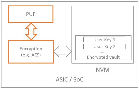
Figure 1. Implementing a highly secure key vault with a PUF
Software IP protection
Some algorithms, such as those applied for medical diagnosis or vital signs measurement, are the results of years or research and development. Hence, they are extremely valuable assets deserving strong protection. PUF generated keys can protect these software IPs through encryption.
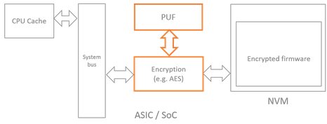
Figure 2. PUF based software IP protection
Device authentication
One of the very first security requirements for connected devices is authentication, that is to say making sure the unit is genuine. The most secure way is to perform challenge – response authentication. In this scheme a random number – the challenge – is sent to the device to be authenticated and the said device signs the challenge with its private key. Here again, the private key must be strongly protected.
PUF Principle
A turnkey solution for implementing secure storage while providing a higher level of protection than traditional techniques - which involves custom design - may sound like the security Graal. We will see that robust and easy to integrate PUF is now a reality.
PUFs rely on minuscule manufacturing variations. The manufacturing variations result in devices mismatch. The idea is that two (or more) devices that are identical by design will actually have different electrical characteristics. The difference in the electrical characteristics is unpredictable and cannot be estimated through observation, neither optical, nor SEM.
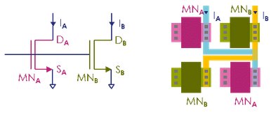
Figure 3. Schematics and laytout views of a transistor pair as a PUF element
In the above schematic, although the two transistors A and B are identical by design, they always have in practice slightly different physical characteristics. Parameters such as threshold voltage (VT), drain-source current (IDS) or drain-source resistance (RDSON) are different. Designers may choose different parameters to build their PUF. In order to stay generic in this paper we will refer to "parameter" PA and "parameter" PB, keeping in mind that it could be any transistor parameter or a combination of them.
As transistors A and B are identical by design, it is impossible neither by simulation nor reverse engineering to predict for each structure whether we will have PA > PB or PA < PB. If we arbitrarily decide that PA > PB generates a “0” and PA < PB a “1”, it is then impossible to guess whether the pair will generate a “0” or “1” when sensed. By repeating our structure N times we can generate an unpredictable stream of N bits. We have just designed a Physical Unclonable Function.
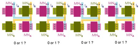
Figure 4. Multiple instances of the transistor pair create an un predictable bit stream
PUF Challenges
As illustrated, implementing a series of multiple instances of our transistor pair, or any other device, is trivial. Thus it might seem very easy to build a PUF based on this principle. Actually it is not!
As said in the introduction, PUF is based on the minuscule variations in silicon manufacturing. In our example this translates into PA > PB or PA < PB. However, because the manufacturing variations are minuscule, so is the difference ΔP = PA - PB . Because ΔP is small, it has to be measured with high accuracy. If not, a "0" could easily flip to "1" or vice-versa and the PUF becomes unusable for key generation. Measurement accuracy is thus a major challenge.
Even worse, ΔP is generally sensitive to aging, as well as temperature, process and power-supply variations. ΔP is by nature small but also randomly distributed, hence cells having the lowest ΔP have a tendency to flip when used at different temperatures. We can consider these cells as "weak" while those having higher ΔP as "strong", the latter being less sensitive to variations. Adding extra or redundant cells as this is done in memory designs is a possible path to replace the weak cells by strong ones.
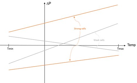
Figure 4. Behavior of "weak" and "strong" cells
While implementing the PUF elements is relatively straightforward, getting stability over said parameters is a real challenge. There are several techniques to build stable PUFs:
- Choose the parameters (VT, IDS, RDSON) so that there easily measurable with high-accuracy;
- Redundancy: design more PUF elements than needed and eliminate the "weak" instances. Here again the number of weak cells need to be thoroughly estimated. Having not enough cells would create yield issues while adding too many redundant cells can make the PUF too large in terms of silicon area. Both would increase the actual die cost.
- Error correction: assuming the percentage of unstable cells is low enough, implementing a proper error correction mechanism such as Hamming coding would "repair" the key. The limitation is that one needs to have a pretty strong estimate of the potential defective PUF units
On top of the measurement accuracy, what makes a PUF solution value are indeed the cost of efficiency of the error correction or redundancy schemes.
Reliability is essential but also as for other key generation processes, one expects for the PUF unpredictability and uniqueness. Unpredictability means that on a given die, even knowing the PUF response to a set of challenges, one cannot guess the response to the next challenge. Uniqueness is the capability for a given PUF design to generate a unique response for each die and for the same challenge [3].
INVIA PUF: a flexible, reliable, secure solution
Architecture
Our PUF is based on the transistor mismatch and includes key diversification. An instance provides 128 security bits and can generate multiple keys thanks to a proven diversification process.
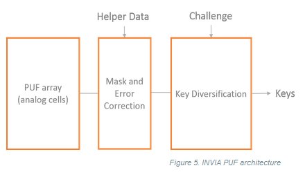
Figure 5. INVIA PUF architecture
Aging resilience
| Aging Phenomena | Description | Impact on INVIA PUF | Impact on other technologies |
|---|---|---|---|
| Hot Carrier Injection (HCI) | Carriers trapped in gate dielectric of NMOS transistors generate Vt and gm shift. | Less than 1% Vt and gm variation on PUF transistors for 10 years at 125°C | Moderate if transistors operate at low Vds significant for switching NMOS at high Vds |
| Time-Dependent Dielectric Breakdown (TDDB) | Oxide breakdown is caused by electron tunneling current | Very limited because our PUF cells operate at ~ 0.5 Vdd max | Significant when MOSFET transistors are operating close to maximum specified operating voltage, limited if not. |
| Negative-Bias Temperature Instability (NBTI) | Vt and gm shift due to positive charges trapping at the oxide-semiconductor boundary underneath the gate. This phenomena can occur when Vg < Vs, it is prevalent in switched-on PMOS transistors | No impact because:
| SRAM based PUF technologies are sensitive to NBTI because they use PMOS transistor with Vg < Vs |
The table above shows our PUF is naturally resilient to aging. To get an even higher level of reliability, we have implemented redundancy: as previously explained we implement more cells than required and eliminate the weak cells. The model we have established for the PUF has allowed us to set-up the right discrimination threshold to eliminate the unreliable PUF elements. Experiments have confirmed the model as well as high temperature operating life test (HTOL). The analog structure enables parameter drift measurement after aging, this gives a much higher level of confidence than a go-no go testing.
Furthermore, the PUF transistors are powered only when sensed meaning for extremely short durations. This naturally reduces the level of stress compared to implementation where the PUF structure such as a memory array is permanently powered.
Entropy
Rather than eliminating weak cells, other implementations build helper data to get robustness against external parameters variations and aging. This may result in a loss of entropy.
INVIA PUF shows an excellent entropy > 0.998 measured on 1.7 billion bits
Modelling
At INVIA, we have designed our PUF IP not only to be robust against temperature, voltage and process variations but also to be able to model it, avoiding any kind of black magic. Because PUF intrinsically relies on pretty random phenomena, one could be tempted to implement PUF cells, run experiment and characterization and if it works empirically release the IP. This might work but not provide the highest level of trust.
Having a PUF model brings significant advantages:
- The solution is trustable. Being sure that the key can be built with a sufficient level of entropy and robustness is very fundamental
- Porting the solution to a different process node is made easier as the result is predictable
- The IP can get certified
Conclusion
Implementing a PUF IP with a guarantee of reliability, unpredictability and uniqueness enables the highest level of security for an ASIC or SoC, even for designers who are not security experts.
References
[1] e. a. S. Quadir, «A survey on chip to system reverse engineering,» ACM Journal on Emerging Technologies in Computing Systems, April 2016.
[2] D. F. M. M. T. Q. S. Huanyu Wang, «Probing Attacks on Integrated Circuits: Challenges and Research Opportunities», IEEE Design & Test , October 2017.
[3] M. Bhargava, «Reliable, Secure, Efficient Physical Unclonable Functions. Thesis», 01 May 2013. [Online]. Available: https://doi.org/10.1184/R1/6721310.v1.
Related Semiconductor IP
- PUF FPGA-Xilinx Premium with key wrap
- PUF FPGA-Xilinx Base
- ASIL-B Ready PUF Hardware Premium with key wrap and certification support
- ASIL-B Ready PUF Hardware Base
- PUF Software Premium with key wrap and certification support
Related White Papers
- Understanding the LIN PHY (physical) layer
- Understanding the Importance of Prerequisites in the VLSI Physical Design Stage
- IC Physical Design: Portable Layout and Simulation Technigues for ADSL Analog Devices
- SOC: Submicron Issues -> Large PLDs need own physical models
Latest White Papers
- Breaking the Memory Bandwidth Boundary. GDDR7 IP Design Challenges & Solutions
- Automating NoC Design to Tackle Rising SoC Complexity
- Memory Prefetching Evaluation of Scientific Applications on a Modern HPC Arm-Based Processor
- Nine Compelling Reasons Why Menta eFPGA Is Essential for Achieving True Crypto Agility in Your ASIC or SoC
- CSR Management: Life Beyond Spreadsheets