System CoreWare Based Design using RapidChip Platform ASIC
Milpitas, CA. USA
Abstract:
Growing design complexities and reduced time to market goals for new products are forcing designers to seek new and innovative ways of managing complexity. Key factors contributing to complexity of a custom integrated circuit (IC) development are: (i) the ability to make effective use of the basic silicon building blocks, (ii) ease of use, accuracy and predictability of the development flow, and (iii) the ability to effectively reuse intellectual property (IP) functions.
With the RapidChip platform LSI Logic effectively addresses these challenges. This paper provides an overview of the RapidChip silicon platform and associated RapidWorx™ design flow. It also shows how System CoreWare solutions enable effective IP reuse.
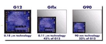
It is well known that smaller process geometries are enabling designers to pack more and more gates onto the same piece of silicon. When moving from one process technology node to the next, designers get approximately 50% additional chip real estate on the same die size. This is illustrated in Figure 1 using LSI Logic’s process technology roadmap.

Figure 1. LSI Logic process technology roadmap
Overall system cost, performance, and power tradeoffs, as well as the need to differentiate push system and chip architects to higher levels of integration enabled by each new process technology node. In addition, time-to-market pressures brought about by shortened market windows and reduced visibility are forcing companies to reduce the overall development time in bringing new products to market.
Unfortunately, as illustrated in Figure 2, the gap between designer productivity and the growth of the number of available transistors on an IC continues to widen. To fully exploit gains from higher levels of integration while meeting time-to-market goals, design productivity has to be improved fundamentally, not incrementally.

Figure 2. Growing Productivity Gap
As described earlier, the key factors that contribute to a design team’s productivity in developing custom integrated circuits are: (i) effective use of the basic silicon building blocks, (ii) ease of use, accuracy and predictability of the development flow, and (iii) the ability to effectively reuse IP in significant portions of the design.
LSI Logic has attacked the problem in all the above-described areas and is enabling designers to realize complex custom ICs in record time. The RapidChip silicon platform, along with its associated RapidWorx design system, address the first two factors in a fundamentally new and innovative manner. CoreWare and System CoreWare IP solutions address the third factor.
RapidChip Silicon Platform
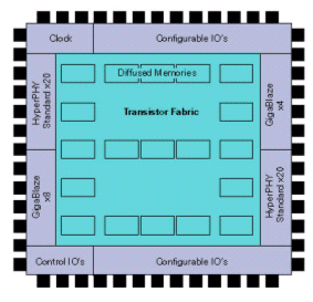
RapidChip designs are based on slices that provide fundamental building blocks such as configurable transistor fabric, memories, I/Os and key IP blocks such as high-performance microprocessor and serializer/deserializer (SerDes) cores from LSI Logic’s CoreWare IP library. The I/O ring is made up of configurable and dedicated I/Os for specific requirements. With the key building blocks defined, slices are manufactured up to the point of metallization. A high level representation of a RapidChip slice is shown in Figure 3.

Figure 3. High-level RapidChip Slice representation
Designers can leverage the pre-defined resources available on slices and personalize them by metallizing the slice to create the complete custom ICs, which meet their end application requirements.
Since slices provide a partially complete IC, there are many benefits to using them as a starting point. These benefits include significant reduction in design and manufacturing times, as well as major savings in the upfront NRE costs, which have been sky-rocketing as we move to newer and smaller process geometries. More significantly for designers, when starting with pre-defined RapidChip slices, the number of development steps to design and verify a custom IC are significantly reduced. Such simplification is achieved without compromising the complexity of the design in terms of the number of gates, memories or in IP use. Further efficiency and simplification is achieved from the RapidWorx design flow specifically created for RapidChip designs. This is described in the next section.
RapidWorx Design System
To ensure fast and predictable design turn-around-times, RapidWorx provides a robust and affordable design system for implementing RapidChip devices. To achieve this, RapidWorx provides a seamless design flow which incorporates rule-based methodology and automated correct-by-construction tools. In addition, many design integrity issues are addressed upfront during slice creation. This simplfies the development flow designers go through when using slices as a starting point for their design. A high level overview of the RapidWorx design flow is illustrated in Figure 4.

Figure 4. RapidWorx Design Flow
RapidWorx design flow eliminates iterations requiring RTL as well as gate level redesign because of timing closure issues during physical design. Since such issues are typically found late in the design flow, addressing them upfront reduces development time as well as costs. RapidWorx guides designers through the various design steps including automated configuration of memories, I/Os, clocks, test insertion, slice resource mapping, RTL rule checking and analysis, physical synthesis, and finally design handoff rule checking.
Key to accomplishing first-pass physical design success is that the inputs to the physical design process, i.e. the design netlist and timing constraints, meet a set of pre-defined criteria. Such criteria guarantee that the required design performance is met and the design structures can be implemented within the available physical resources of the selected RapidChip slice.
RTL analysis, a key component in this flow, identifies implementation unfriendly structures that might correctly describe the required functionality, but which cause problems in the physical design process. Identifying such structures early in the design process allows RTL changes to be made upfront, thereby eliminating the need for iterations during the physical design phase.
Armed with RapidChip slices and an easy-to-use and predictable RapidWorx design system, custom IC designers can further manage complexity by leveraging System CoreWare IP.
System CoreWare IP Solutions
Over a decade ago, LSI Logic’s pioneering efforts in IP reuse revolutionized ASIC design by establishing a proven CoreWare IP portfolio. CoreWare set the standard in the industry with its rich set of proven, easy to integrate, and performance-leading IP cores. LSI Logic recently introduced System CoreWare IP that extends its IP platform capabilities.
System CoreWare IP combines multiple CoreWare IP functions into pre-integrated, pre-verified systems. By raising the level of IP integration and abstraction from component IP blocks to pre-defined systems, the risk and design time associated with developing complex custom system on a chip (SoC) designs is significantly reduced. When using System CoreWare IP, designers no longer need to spend valuable development time building and verifying commonly used IP subsystems. Instead, they can focus their energies on differentiating logic or secret sauce for their end application.
One such System CoreWare solution is based on the popular ARM926EJ-S processor core. The
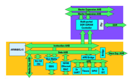
ARM926 System CoreWare IP provides a rich set of pre-defined peripherals, extendable bus structures, and an extensive verification environment. A block diagram of this system is shown in Figure 5.
The processor system consists of multiple proven CoreWare IP functions such as ARM926EJ-S processor core, Ethernet controller, vectored interrupt controller, UARTs, GPIOs, IIC, and an external bus interface unit (EBIU) that also serves as a static memory controller. This system provides all the hardware functions needed to run popular operating systems.

Figure 5. ARM926EJ-S processor system block diagram
The system is designed as a fixed function that can be extended by designers at predefined expansion interfaces. These expansion interfaces are based on the industry standard AMBA on-chip bus and allow designers to easily integrate their own value-added logic or cores from LSI Logic’s CoreWare IP library such as the multi-ported DDR SDRAM memory controller. This is shown in Figure 6.

Figure 6. Multi-ported DDR SDRAM memory controller integrated with the processor system
To enable easy expansion and seamless integration of System CoreWare IP functions with the rest of the custom IC, designers are provided with an extensive but easy to use system verification environment. By exposing an industry standard on-chip bus architecture at the expansion interfaces of the system, designers can also leverage the wealth of available 3rd party verification IP components, such as transactors, monitors, and checkers, available for AMBA.
A significant portion of the overall product development time, especially with processors based SoCs, is spent in software development. By basing the subsystem around an industry standard processor architecture, designers can leverage the broad availability of standard ARM software development tools.
Additionally, fixing and encapsulating the hardware components required by popular operating systems such as interrupt controllers, timers, etc. within the processor subsystem itself enables creation of standard board support packages (BSP). These standard BSPs are reusable across multiple designs and applications as they are based on common hardware components. LSI Logic has partnered with 3rd party software vendors to provide BSP solutions for popular operating systems such as Linux and VxWorks. Finally, to enable application software development prior to silicon availability of the custom IC, a software model providing fast full-function software emulation of the ARM926 System CoreWare IP is available. The software model can be extended by designers to include additional application specific logic.
Key to designing successful System CoreWare IP, sometimes referred to as IP platforms, is maintaining the balance between reusable IP and what the end-application designers may consider as differentiating IP. It is not uncommon to see IP platforms gain limited adoption when they tend to encroach into portions of the design that are considered to be differentiating by end-application designers. System CoreWare solutions address this balance well in the way they are constructed. A simple example that illustrates this well is the IP composition of the ARM926 System CoreWare solution.
As shown in Figure 5, although the memory interface used for booting (EBIU) is encapsulated within the processor system, the main memory interface is not included. The processor system exposes a standard AMBA AHB bus for designers to connect the memory interface that best suits their application performance and cost targets. Such a memory interface solution could be selected from the CoreWare library or designers can develop their own if there are special requirements or a need for differentiation. A System CoreWare based solution for DDR SDRAM is connected to the processor subsystem as shown in Figure 6. Key to being successful with this modular approach is the ease with which designers can connect the different systems or extend around them. This is where CoreWare and System CoreWare IP stand out.
One can easily envision other System CoreWare solutions based around memory interfaces i.e. I/O and Phy along with the associated memory controller or a high-speed SerDes along with the associated link and protocol layer IP such as 4 lanes of 2.5Gigbit SerDes with PCI-Express link and protocol layer IP. Such easy to use high-speed protocol specific “pipes” encapsulate the complex signaling issues internally and expose clean digital and standardized on-chip interfaces, such as AMBA AHB or AXI, to designers. This allows designers to focus on their value-add logic for managing and shaping data from these “pipes” per the application needs rather than spending time implementing the “pipe” itself. The higher-level abstraction of IP functions allows designers to manage complexity much better in today’s multi-million gate ICs.
Summary and Conclusions
As design complexity and the gap in productivity with pre-existing design capabilities increases, designers must employ fundamentally new mechanisms to manage complexity and meet shortened time to market goals for each new product. Design complexity is a multi-dimensional problem. As outlined in this paper, the fundamental factors influencing complexity when developing complex custom ICs are: (i) effective ability to use the basic silicon building blocks, (ii) ease of use, accuracy and predictability of the development flow, and (iii) the ability to effectively reuse IP functions.
Many solutions address just one or two of these factors, but LSI Logic with a combination of the RapidChip silicon platform, the RapidWorx design system, and the System CoreWare IP solution effectively addresses all three factors. This complete solution is driving a new way to develop complex custom ICs with significantly reduced development time and cost.
By raising the level of abstraction from component IP to pre-defined, pre-verified systems that are modular and easily extendable, System CoreWare IP significantly improves the level of productivity. Designers can now focus their energies on the differentiating portions of their ICs and develop a new wave of innovative semiconductor chips.
References
[1] RapidChip Technology Fast Custom Silicon through Platform-Based Design White Paper at www.lsilogic.com/rapidchip
Related Semiconductor IP
- DeWarp IP
- 6-bit, 12 GSPS Flash ADC - GlobalFoundries 22nm
- LunaNet AFS LDPC Encoder and Decoder IP Core
- ReRAM NVM in DB HiTek 130nm BCD
- UFS 5.0 Host Controller IP
Related Articles
- The Platform Based SOC Design that Utilizes Structured ASIC Technology
- PCI Express Design Considerations -- RapidChip Platform ASIC vs. FPGA Design Efficiency
- System Performance Analysis and Software Optimization Using a TLM Virtual Platform
- Aircraft Jet Engine Failure Analytics Using Google Cloud Platform Based Deep Learning
Latest Articles
- TensorPool: A 3D-Stacked 8.4TFLOPS/4.3W Many-Core Domain-Specific Processor for AI-Native Radio Access Networks
- Assertain: Automated Security Assertion Generation Using Large Language Models
- VolTune: A Fine-Grained Runtime Voltage Control Architecture for FPGA Systems
- A Lightweight High-Throughput Collective-Capable NoC for Large-Scale ML Accelerators
- Quantifying Uncertainty in FMEDA Safety Metrics: An Error Propagation Approach for Enhanced ASIC Verification