Recent progress in spin-orbit torque magnetic random-access memory
By V. D. Nguyen, S. Rao, K. Wostyn & S. Couet - imec
Abstract
Spin-orbit torque magnetic random-access memory (SOT-MRAM) offers promise for fast operation and high endurance but faces challenges such as low switching current, reliable field free switching, and back-end of line manufacturing processes. We review recent advancements in perpendicular SOT-MRAM devices, emphasizing on material developments to enhance charge-spin conversion efficiency and large-scale device integration strategies. We also discuss the remaining challenges in achieving a single device with low switching current, reliable field free switching to unlock the full potential of SOT-MRAM technology.
Introduction: Value proposition of SOT-MRAM
The miniaturization predicted by Moore’s law has driven the evolution of electronic devices, leading to the explosive growth of our digital society as today1. However, as we continue to advance high-performance computing and energy efficiency, traditional charge-based memory technologies such as Static Random-Access Memory (SRAM) encounter significant challenges, primarily stemming from leakage current and limited density scaling, especially as the industry transition to the nanosheet transistor era1.
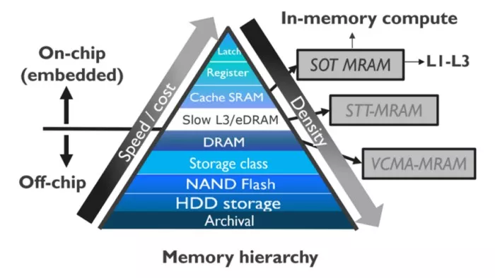
Magnetic random-access memory (MRAM), leveraging the spin properties of materials for data storage, has emerged as a promising solution to the challenges of charge-based memory devices2,3,4,5,6. At the core of MRAM is the magnetic tunnel junction (MTJ), a heterostructure comprising an oxide tunneling barrier sandwiched between the free and pinned layers. In MTJ devices, the magnetization state of the free layer serves to store bits of information, while the magnetization state of the reference layer remains fixed. Over the years, MRAM technology has seen significant advancements, boosting the scalability and performances2,3,4. With its non-volatility, fast read/write speeds, and high endurance, MRAM holds the potential to replace charge-based memory in various levels of the memory hierarchy (Fig. 1).

Fig. 1: Memory hierarchy presents various types of memory.
MRAM technologies provide promise to replace charge-based memory devices at different cache levels, ranging from L1 to L4. SRAM and DRAM stand for Static Random-Access Memory and Dynamic Random-Access Memory, respectively, while HDD refers to magnetic hard disk drives. SOT-MRAM is aimed at replacing SRAM due to its fast operation, while STT-MRAM is targeted for high-performance and high-density embedded DRAM applications. Voltage-controlled magnetic anisotropy technology offers potential for low-power operation and is being explored as a replacement for DRAM.
While Spin-Transfer Torque (STT)-MRAM has matured, its writing operation where a current is injected through the junction to switch the magnetization orientation of the free layer, faces inherent trade-offs between fast switching speeds and long-term endurance, primarily attributed to the shared read and write current paths.
In response to these challenges, Spin-Orbit Torque (SOT)-MRAM, by employing separated write and read paths, has emerged as a promising alternative to mitigate the challenges associated with fast operation and high endurance in STT-MRAM devices5,7,8,9,10. This unique feature positions SOT-MRAM as a compelling candidate for providing a fast and dense memory alternative to SRAM (at least for the bigger caches), where high performance and reliability are important. Following the industrial trend towards chiplets and 3D integration, high-performance memory dies can be envisioned for 3D integration alongside accelerator processing units.
However, realizing the full potential of SOT-MRAM requires overcoming several critical hurdles such as:
- Integrating perpendicular magnetic anisotropy (PMA) systems is imperative to unlock the scalability potential of SOT-MRAM, aligning it with the evolution of advanced technological nodes.
- Implementing field-free switching mechanisms and achieving low switching currents in PMA systems are also critical for practical application of SOT-MRAM.
- Furthermore, ensuring compatibility with back-end of line (BEOL) complementary metal-oxide-semiconductor (CMOS) fabrication processes is essential for seamless integration into existing manufacturing processes.
To address these challenges, advancements in understanding physics of SOT phenomena, materials research, and device engineering are essential for realizing SOT-MRAM technology. The fundamental physics of charge-to-spin conversion and methodologies for quantifying its efficiency across various material categories, along with SOT induced magnetization switching, have been comprehensively covered in numerous review articles5,9,10,11,12,13. In this review, our primary focus lies on the technological aspects, particularly enabling SOT-MRAM technology through material advancements and device integration strategies.
SOT-MRAM with in-plane MTJs have been demonstrated to be compatible with BEOL processes and enable field-free switching operation14,15. However, achieving further miniaturization and scaling of in-plane SOT-MRAM technology is hindered by specific elliptical shape requirements, limiting their scalability potential.
Therefore, this review delves into recent advancements in perpendicular SOT-MRAM device development, highlighting important technological requirements, progress of material research, large-scale integration demonstrations, and approaches for field-free SOT switching. Ongoing research endeavors aim to achieve BEOL compatibility, ultra-scale cells, and voltage-gated SOT devices in multi-pillar MTJs, thereby addressing the footprint challenges and prospects in SOT-MRAM technology.
To read the full article, click here
Related Semiconductor IP
- NPU IP Core for Mobile
- NPU IP Core for Edge
- Specialized Video Processing NPU IP
- HYPERBUS™ Memory Controller
- AV1 Video Encoder IP
Related White Papers
- MEMS -> MEMS switch uses magnetic actuation
- How to build reliable FPGA memory interface controllers without writing your own RTL code!
- Video content protection using secure embedded non-volatile memory for HDMI with HDCP
- Verification challenges of embedded memory devices
Latest White Papers
- Breaking the Memory Bandwidth Boundary. GDDR7 IP Design Challenges & Solutions
- Automating NoC Design to Tackle Rising SoC Complexity
- Memory Prefetching Evaluation of Scientific Applications on a Modern HPC Arm-Based Processor
- Nine Compelling Reasons Why Menta eFPGA Is Essential for Achieving True Crypto Agility in Your ASIC or SoC
- CSR Management: Life Beyond Spreadsheets