Reducing Power Consumption while increasing SoC Performance
By Gregory Recupero, Performance-IP
Overview
Designers of today's high-performance multi-client SoCs struggle to achieve the best possible performance/watt for their designs. Every generation of product must improve the customer's user experience by delivering more performance. While at the same time battery life must increase with each subsequent product generation. Performance-IP has developed a family of products based on its patent-pending Memory Tracker Technology. This technology enables products to operate at higher levels of efficiency, reducing power consumption while increasing SoC performance.
Design Challenge
To show the effectiveness of Performance-IP’s Memory Tracker Technology a typical SoC Design will be assembled. Then three different approaches will be implemented to improve system performance. The first approach will be to increase the CPU cache size to improve performance. The second approach will be to implement a traditional prefetch engine to reduce memory latency and improve performance. And the final approach will be the use of Performance-IP's Memory Request OptimizerTM. For each of the approaches CPU IPC will be evaluated along with DDR memory power and bandwidth. To maintain consistency between all three design approaches, solutions that have similar silicon area were used to perform the analysis.
Typical SoC Design
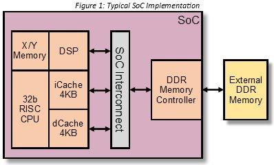
A typical SoC design consists of a CPU, memory clients, interconnect, and a memory sub-system. For our design challenge the SoC implementation used is shown in Figure 1.
Design Approach 1 - Increase Cache Size
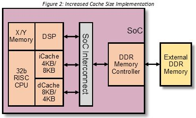
This approach involved increasing the CPU cache sizes from 4KB to 8KB. To maintain consistent silicon area with all our design solutions, the D-cache and I-cache sizes were increased independently. First, the D-cache size was increased from 4KB to 8KB, while maintaining the standard 4KB I-cache. Application performance and DDR power estimates were computed. Then the I-cache size was increased to 8KB, while maintaining the standard 4KB D-cache. Application performance and DDR power estimates were again computed. The increased cache size design approach is shown in Figure 2.
Design Approach 2 - Typical Prefetch Engine
The Prefetch Engine (PFE) approach required the implementation of a linear prefetch look ahead. Its basic operation consisted of monitoring when any of the SoC clients fetched data from memory, then fetching the next sequential (in terms of memory address) cache line and storing it in a 'response buffer' within the PFE. This design approach is shown in Figure 3 below.
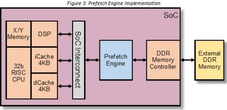
To improve efficiency and performance of the PFE, multiple separate response buffers were implemented to hold the prefetched cache lines. A maximum of 16 response buffers could be implemented without exceeding our design area constraints. Each response buffer contained the address for the cache line of data it contained, along with the entire cache line of data. This allowed the response buffers to operate very similar to a fully associative cache.
Design Approach 3 - Performance-IPs Memory Request OptimizerTM
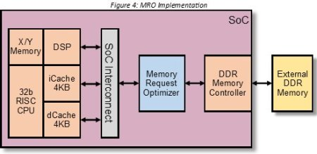
The Memory Request OptimizerTM (MRO) design solution is the next-generation of memory prefetch and is based on Performance-IPs Memory Tracker TechnologyTM. This product shows how the addition of the Memory Tracker TechnologyTM can dramatically improve the efficiency of a memory prefetch engine.
This added efficiency allows the MRO to handle multiple read request streams concurrently, analyzing each client’s request to determine which memory requests will yield optimal results. Since the MRO can be dynamically programmed, a system can be tuned for the required performance needed by the target application. The SoC architecture containing the MRO is shown in Figure 4 below.
The MRO provides four modes of optimization; none, low, moderate, and aggressive. Each mode provides a higher level of performance than the previous mode. The low and moderate modes are designed to produce the best performance/watt solution, while the aggressive mode is meant to be used for achieving the highest possible performance.
SoC Application
To demonstrate how each of the design solutions above improves overall processor performance, a baseline system-level Verilog simulation was run using a DDR model with 25-cycles of memory latency. The Verilog simulation was performing a full MP3 audio decode. Two parameters were then obtained from this simulation.
First, the baseline CPU Instructions Executed Per Cycle (IPC) was calculated. A system with lower memory latency will achieve higher processor IPC, since the processor pipeline won't stall as often while waiting for a data or instruction fetch. This parameter allowed us to measure the performance improvement.
The other parameter recorded was the total number of reads that reached the external memory. Since our design goal is to produce the best performance/watt solution, fewer external reads translates to less system power. This is because every read that reaches external memory consumes approximately 10x more energy than if that same read had occurred on-chip. To monitor this parameter, the number of reads to external memory that each design solution generated to decode the MP3 stream was tabulated. The goal of each design solution would be to generate the highest IPC improvement, but not at the expense of generating additional reads to external memory.
Results
The simulation results for each of the design approaches are reviewed below.
Increasing Cache Size - Results
Doubling either the I-cache or D-cache size resulted in the fewest reads to external memory; however they produced the smallest IPC improvements. This is shown in the table below.

It should be noted that doubling the D-cache size produced better results than doubling the I-cache. This is most likely due to the data changing over time (exhibiting a high degree of temporal locality). Since increasing the D-cache produced better overall results, only the D-cache results will be used to compare against the other designs approaches.
Adding a Prefetch Engine - Results
Adding a prefetch engine generated the largest reduction in memory latency, and resulted in the highest IPC improvement. This increase in IPC however did come at high cost. The PFE dramatically increased the number of reads to external memory. The prefetch engine generated a 22.8% increase of reads to the external memory during the execution of the MP3 decode application. This is because the PFE is fetching data that is not needed. These additional reads consume more power, and increase the required memory bandwidth. It was our goal to reduce both of these constraints. To see if the prefetch engine could overcome this problem additional simulations were run doubling the number of response buffers to 32 and doubling again to 64. This only reduced the number of external reads to 21% and 18.5% respectively, without appreciable IPC improvements. This confirms the excessive false fetches being performed by the PFE. This data is shown in the table below.

Memory Request OptimizerTM Results
The MRO analysis was performed for each optimization mode. The low and moderate optimization modes generated large reductions in latency which translated in to solid IPC improvements. Both of these modes performed very well and they did not generate any extra reads to memory, in fact the total number of external reads were reduced. The aggressive optimization level results actually approached those of the prefetch engine while generating fewer total reads to external memory. The MRO results are shown in the table below.

Power Savings Results
Our design goal is to produce the best performance/watt design. With these improvements in performance we can reduce the processor clock rate and maintain the same level of processing. Reducing the processor clock rate will also reduce the dynamic power consumption of our designs. If we use the equation for the dynamic contribution to power we have:
Pdynamic = σCV2f
In this equation σ is the activity factor or the portion of the circuit switching, C is the total switching capacitance, V is the voltage, and f is the switching frequency. Because the design is not changing σ and C will be the same. If σ, C, and V are constant, and any reduction in frequency will result in a proportional reduction in dynamic power.
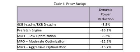
Based on the processor IPC performance improvements noted in Tables 1 - 3, we can reduce the SoC clock frequency to maintain the same application performance as the baseline. This will result in a reduction of power consumption between 5 - 16%, as shown below in Table 4.
A more aggressive power reduction approach would also involve voltage-scaling, because of the squared contribution of voltage to dynamic power consumption. Designs that have lower clock rates can achieve high voltage-scaling. This is another benefit from reducing the required clock rate.
Finally the DDR power reductions were analyzed. One of the design goals was to reduce the number of reads that reached the external memory sub-system. For this analysis the baseline simulation was used to determine the percentages of time spent in each of the various DDR states, and compute a power estimate based on this data. This was then repeated for each of the different designs.
Designs that ran faster would also spend more time in the low power DDR states further helping to reduce power consumption. The results for each of the designs are shown below in Table 5.
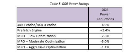
The D-cache performed best here because of the large reduction in external DDR reads. Second, was the Memory Request Optimization approach using moderate optimization mode.
What was not expected was the MRO aggressive optimization which ended up consuming less DDR power than the baseline simulation. This was because of the large performance boost generated by this design which allowed the DDR to ultimately spend more time in the lower power states. This power reduction was just enough to overcome the extra power spent performing the additional 7.8% of reads. This was also true for the prefetch engine solution which only consumed an additional 3.4% of DDR power. This was much less than anticipated, but the power saved could not suppress the power expended performing the additional 22.8% of reads, not to mention the required increase in memory bandwidth.
Design Challenge Winner
All three design approaches produced reductions in application latency reductions. Only the prefetch engine and the MRO design solutions translated these latency reductions in to appreciable IPC improvements. However the additional memory bandwidth increase from the prefetch engine made that solution unacceptable. The two approaches that contributed appreciable improvement in IPC and power reductions, while generating fewer reads to the memory sub-system were the low and moderate optimization methods of the MRO. The moderate optimization provided the largest dynamic power savings, combined with the 3% reduction in DDR power making it the clear performance/watt winner.
Conclusion
The results from this Design Challenge shows that the incorporation of the Memory Tracker TechnologyTM can improve the efficiency of the Memory Request OptimizerTM. This allowed it to outperform both the cache and prefetch engine design solutions. This same Memory Tracker TechnologyTM has also been incorporated in to Performance-IPs L2+ Cache solution. This allows our cache solution to warm faster and achieve higher hit rates than level2 cache designs of the same size. In fact our L2+ Cache has outperformed some caches that are up to 4 times as large. So to save power without sacrificing performance check out the products offered by Performance-IP.
Related Semiconductor IP
- Ultra-Low-Power LPDDR3/LPDDR2/DDR3L Combo Subsystem
- 1G BASE-T Ethernet Verification IP
- Network-on-Chip (NoC)
- Microsecond Channel (MSC/MSC-Plus) Controller
- 12-bit, 400 MSPS SAR ADC - TSMC 12nm FFC
Related Articles
- Reducing IC power consumption: Low-power design techniques
- NoC Interconnect Fabric IP Improves SoC Power, Performance and Area
- Achieving Lower Power, Better Performance, And Optimized Wire Length In Advanced SoC Designs
- Optimize performance and power consumption with DSP hardware, software
Latest Articles
- Extending and Accelerating Inner Product Masking with Fault Detection via Instruction Set Extension
- ioPUF+: A PUF Based on I/O Pull-Up/Down Resistors for Secret Key Generation in IoT Nodes
- In-Situ Encryption of Single-Transistor Nonvolatile Memories without Density Loss
- David vs. Goliath: Can Small Models Win Big with Agentic AI in Hardware Design?
- RoMe: Row Granularity Access Memory System for Large Language Models