Quantum Tunneling Mechanism in NeoFuse
By eMemory Technology Inc.
NeoFuse is a logic-process compatible non-volatile memory (logic-NVM) using impedance change for data storage in one-time programming (OTP) applications. Storing data through NeoFuse can enable low-power operation, high reliability, and strong security. Using NeoFuse OTP IP as an embedded memory solution in a chip will provide user-friendly interface and fully integrated OTP IP that minimizes design effort and circuit complexity.
The NeoFuse OTP IP can be used for: (1) code storage, (2) identification or encryption data storage, (3) storage of timing, parameter setting, function selection, (4) and flexibility of field updates and product customization. Therefore, NeoFuse macros suits a wide range of applications, including set-top boxes, application processors, digital TVs, CMOS imaging sensors, baseband processors, LCD drivers, power management ICs and more.
The judgement on data “0” or data “1” relies on the gate conduction current level of a core nFET within the NeoFuse cell. The initial state of a NeoFuse bit-cell shows high impedance in the gate oxide because the trap density of the gate oxide is extreme low. To write data, the impedance of the gate oxide can be changed through programming with a well-chosen gate bias. After programming, the gate conduction current will significantly increase. The sensing amplifier in the NeoFuse macro can distinguish whether the memory bit stays at data “1” or data “0”.
To generate a high gate conduction current in a thick-oxide FET, a percolation path must be created under the high gate electric field for the gate current to move through this percolation path. However, the conducting mechanism in ultra-thin gate oxide is quite different. The main conducting mechanism is quantum tunneling in the ultra-thin gate oxide.
Classic mechanics predict that particles with insufficient energy cannot surmount an energy barrier. However, a proportion of particles can actually penetrate an energy barrier even if all particles do not have enough energy. Quantum mechanics predict a non-zero probability of a particle to be on the other side of the energy barrier because every particle has wave-particle duality in nanoscale or quantum-scale.
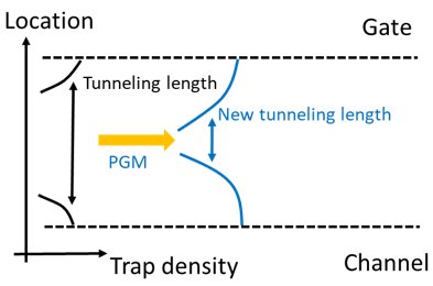
When voltage is applied to the gate oxide of a NeoFuse bit-cell, the high electric field will be built across the gate oxide and generate dangling bonds. The corresponding trap density will increase as the programming process continues. Thus, the trap density is exponentially distributed near one or both interfaces after programming.
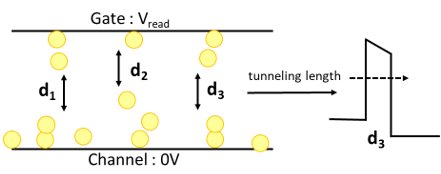
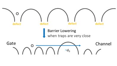
When this high-density traps at both interfaces are very close and the electrons from the channel can tunnel directly through this narrow forbidden energy barrier in the gate oxide, this process is a direct tunneling process. This tunneling phenomenon is due the reduction of the effective tunneling length after the programming procedure in the ultra-thin oxide, which is illustrate in Fig. 1 and Fig. 2. The tunneling current on the 40-nm platform can reach over 10 uA as the tunneling length decreases to 10 Angstrom in the programming operation of the NeoFuse bit-cell.

Fig. 1: The tunneling current is huge as the trap density increases.

Fig.2: The barrier height lowers when the trap density increases. In addition, the tunneling length is also reduced significantly.
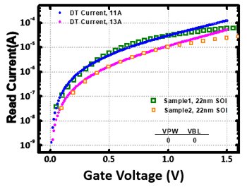
Fig. 3 illustrates the trap distribution of the ultra-thin oxide in the programming operation. After applying voltage in an ultra-thin oxide, the tunneling length will be reduced, creating a large trap-rich oxide area. The direct tunneling model is expressed as equation 1 [1]. Fig. 4 is the comparison between the direct tunneling model and the experiment results of the 22nm SOI platform. The simulated current using the direct tunneling model supports the experimental result. The discrepancies between the simulated and measured data in Fig. 4 may be caused by the parasitic resistance at gate bias > 1V.

Where A and B are physical parameters [1].

Fig. 3: The trap density is exponentially distributed near one or both interfaces after programming or bias stressing. When this high-density traps at both interfaces is very close, the electrons from the channel can tunnel directly.

Fig. 4: The simulated current using the direct tunneling model supports the experiment.
The conducting mechanism of NeoFuse bit-cell is based on quantum tunneling. The tunneling length of NeoFuse bit-cell is controlled through biasing a well-chosen high voltage. On the other hand, when technology keeps scaling down to advanced nodes, the gate oxide will become thinner and further facilitate the direct tunneling. Since the conduction is based on trap generation, the conduction path is invisible against the most advanced inspector (such as TEM and SEM). It is very hard to visually extract the secret stored in NeoFuse OTP by using invasive security attacks. Therefore, NeoFuse can serve as a high security solution. Furthermore, from the literature, the dangling bonds need at least more than 600-700 degree Celsius for recovery. This means the NeoFuse can perform high reliability applications and be used as an automotive grade OTP IP.
[1] Chang-Hoon Choi, Kwang-Hoon Oh, Jung-Suk Goo, Zhiping Yu, and Robert W. Dutton, “Direct Tunneling Current Model for Circuit Simulation, “ International Electron Devices Meeting 1999. Technical Digest (Cat. No.99CH36318).
Related Semiconductor IP
- eFuse Controller IP
- Efuse Switch - GlobalFoundries 130nm RFSOI
- SPI and Efuse - GlobalFoundries 130nm RFSOI
- 3.3V to 2.0V with 288mA driving capability with external capacitor,use trimming ports (need e-Fuse IP); Linear Regulator; UMC 28nm Logic HPC Process
- 3.3V to 1.2V with 150mA driving capability without external capacitor(Cap-less); use trimming ports (need e-Fuse IP); Linear Regulator; UMC 55nm eFlash LowK Logic Process
Related Articles
- The Quantum Tunneling Mechanism of NeoPUF
- NeoPUF, A Reliable and Non-traceable Quantum Tunneling PUF
- Opto-electronics -> Quantum wells integrate optical devices
- Tunneling SPI-4.2 Through an Advanced Switching Fabric
Latest Articles
- A Scalable Open-Source QEC System with Sub-Microsecond Decoding-Feedback Latency
- SNAP-V: A RISC-V SoC with Configurable Neuromorphic Acceleration for Small-Scale Spiking Neural Networks
- An FPGA Implementation of Displacement Vector Search for Intra Pattern Copy in JPEG XS
- A Persistent-State Dataflow Accelerator for Memory-Bound Linear Attention Decode on FPGA
- VMXDOTP: A RISC-V Vector ISA Extension for Efficient Microscaling (MX) Format Acceleration