Secure Your Security Key in On-Chip SRAM: Techniques to avoid Data Remanance Attacks
Noida, India
Abstract :
Security protection in modern microcontroller’s logic devices with memories is based on the assumption that information from the memory disappears completely after erasing or when the power to the memory is removed. After information in memory is erased there may be some physical characteristics of the memory that allow erased data to be reconstructed. Data Remanence poses a serious threat to widespread applications that support this security protection assumption. This paper presents the effects of Data Remanance and techniques to avoid Security Key retrieval by data remanence attacks.
Problem with Data Remanance
Generally Crypto processors/accelerators repeatedly feed a private key through the same circuit that may be programmed in on-chip SRAM (Static Random Access Memory) that is the most commonly used volatile memory in microcontrollers.
Data remanence is the residual physical representation of data that has been in some way erased. Contrary to common wisdom, the SRAM memory cells do not entirely loose the contents when power is cut. This is due to the physical properties of the semiconductor caused by Electromigration, Hot Carriers and Ionic contamination. So a Key that was stored in the same SRAM cells over a long period of time eventually gets “burned” into the memory cells and there is a high probability that key value is retained even after switching off the device.
Data retention in SRAM is also significantly increased with lowering the operation temperature of the SoC. Data may be retained for around 1 ½ hours at 75°C, 3 days at 50°C, nearly two months at 20°C, and approximately 3 years at 0°C.
This poses a serious threat to hardware which operates with secret information (typically “Security Key”) in a secure environment.
Data Remanance Attacks
There may be a physical attack on a chip to investigate the chip design in order to get information about proprietary algorithms or to determine the secret keys by probing points inside the chip. Hence, this attack targets parts of the Chip, which are not available through the normal I/O pins. This can potentially be achieved through visual inspections by using tools such as optical microscopes and mechanical probes. An attacker may even use sophisticated technique like Focused Ion Beam workstation (FIB) or a high end Electron-Beam Tester (EBT) to launch such an attack. To conclude a physical attack against SRAM can be launched successfully assuming the above techniques can be transferred. However, the physical attacks are quite costly and having the structure and the size of an SoC, the attack will probably only be possible for large organizations like intelligence services.
A User Scenario on Remanance Attack
Figure 1 shows Processor local memory, connected to the processor or CPU on one side and to the system bus on the other side.
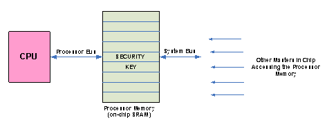
Figure 1 : Processor Memory Connectivity with the core and the system
A low end microcontroller application that chooses to use a Static or Symmetric key for an application may want to store it in a fixed location (for the sake of simplicity) as shown. When the system is up, typically a secure application is protected by tampering features that senses change in pressure, temperature etc such that when such a condition occurs( for example attacker trying to break open the device by applying pressure) tampering logic gets activated and takes the necessary action(easing complete memory so that attacker cannot retrieve any information). So it is highly unlikely that an attacker will try to extract information or perform a physical attack when the system is up and powered. However attacker may choose to remove the power of the system so it de-activates the tampering logic. Assuming Data/Key in SRAM is retained for sufficient amount of time once the power is switched off due to Remanance effort, attacker may just probe the SRAM(using techniques described above) to read the information and extract the Security key.
A real world application for the above attack may be security module used in a bank that manages the Personal Identification Numbers (PINs) issued to costumers for use with ATM’s.
The PIN is derived from the account number by encrypting it with a ’PIN key’, decimalizing the result and adding a decimal ’offset’ to get the PIN the customer must enter. All these cryptographic operations, plus the associated key management operations, are performed in trusted hardware, so that no single bank staff employee has access to a costumer PIN.
As ATM’s need servicing every few years to change the battery (thus power being removed from the secure system), the master keys are loaded back in afterwards by trusted bank staff. Due to memory remanance effect it is highly likely that during the time battery is removed (system being powered off), master keys are retained and can be recovered (by techniques described in previous section).
Paper by Kuhn and Anderson [2] describes in great detail the above scenario where they looked at an ATM that dated from the late 1980’s, and found that the master key values were almost intact on power-up.
Low Temperature Data Remanance Attacks
In the 1980s, it was realized that low temperatures can increase the data retention time of SRAM to many seconds or even minutes. With the devices available at that time, it was found that increased data retention started about −20°C and increased as temperature fell further [3]. Security Devices are therefore designed with temperature sensors; any drop below −20°C is treated as a tampering event and results in immediate memory zeroisation [5]
Leveraging this concept, a hacker may cool the Chip to an appropriate low temperature, remove the power (this deactivates any tampering logic), open the device, extract the chip and power it up again in order to extract the data that is still there.
Design Techniques to Avoid Data Remanance Attacks in SRAM
The best way to avoid data retention effects is to ensure that no memory cell holds a data value for more than a certain amount of time. One of the ways to do so is to periodically flip the stored bits so that each memory cell never holds a value long enough for it be be remembered. This may be impractical to do so for a large amount of data as it may effect CPU performance, this may be feasible for small amounts of sensitive data such as security keys used in Cryptography algorithms.
This can be implemented as a simple digital logic around an existing encryption function that ensures that the same key bits are never stored in a SRAM cell for more than a certain amount of time (say 5 Minutes). System may choose the value of the timer such that it does not degrade CPU performance yet meeting the requirements to avoid data retention.
Incase of customized circuit (for example in a specialized crypto processor or module), it may be possible to integrate this bit-flipping into the memory circuitry. At each DRAM refresh cycle, the complement of the read value is written. When data is read from the cell, it is XORed with the “variable” which tracks the state of the data currently stored in the cells[6].
Since SRAMs don’t have a DRAM-style refresh cycle, this type of circuit modification isn’t really possible for them, so that performing bit-flipping in an SRAM would require the addition of DRAM-style refresh circuitry, negating most of the advantages of SRAM [6].
Alternatively a solution that doesn’t require complex bit-flipping is moving the data (this may be just the security key) around in memory occasionally and overwriting the original storage locations, again ensuring that data is never stored in a SRAM cell for too long.
Next section describes some of the techniques in details to avoid a data remanance attack.
Avoid Data Remanance Attack: Moving The Keys Periodically
1. Allocate 5-10 times extra space in memory that is normally required to store critical data like secure Key. For instance if the security key consists of a single byte (as shown in Figure2), allocate 5 additional bytes where this key would be moved periodically.
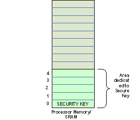
Figure 2 : Secure Key Storage in SRAM
2. Digital Logic will read back the Key after say every N Clock Cycles or Fixed amount of Time.
3. The logic will move the Key from Location 0 to say location 1 every N clock cycles and write the Pattern “10101010” (repeated “1” followed by “0”) to rest of the locations dedicated to secure Key storage(as shown in Figure 3). At the same time a register “Security Key Tracking Register” in the SoC tracks the position as to where the new key is residing.
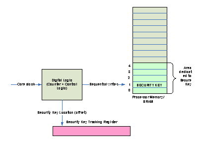
Figure 3 : Digital Logic moving the Secure Key in SRAM
4. When the counter expires again after N cycles, Security Key is again moved from Location 1 to Location 2 but now compliment pattern (“01010101”) is written to the other locations. Key Tracking Register is also updated or incremented to indicate the new key location.
Key tracking registers may not be a complete register but a few bits to indicate the offset for i.e say 3 bit register to indicate 0-5 offset.
The above technique ensures the Memory cell dedicated to Secure Key storage is never burned to the same value and always programmed to different sequence ensuring that no fixed pattern gets stored in the memory. This would prevent Secure Key retrieval during power off as pattern was always dynamic and moving.
Only disadvantage in this technique is the logic overhead and additional SRAM Memory.
Avoid Data Remanance Attack: Program the SRAM with Random Sequencing during Power Off
This technique loads the SRAM with random data before erasing it when the power to the SoC is about to go off.
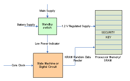
Figure 4 : Random Data generation Logic
Figure 4 shows a typical system that works on Main Supply and Battery Supply. Standby Switch shown generates the regulated supply for the core logic. During the time when the power to the SoC is switched off (Main supply off), Standby Switch generates a low power indicator to the Digital State Machine shown.
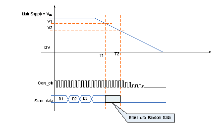
Figure 5 : SRAM erased with random data during Power down sequence
As shown in Figure 5, State Machine starts writing the following sequence on CPU Clock as it gets the indication from the Standby Switch that power is about to go off.
- Write all one’s
- Write all zero’s
- Repeat 1 & 2 several times (programmable by State Machine)
- Finally erase all data in KRAM.
The above sequence also ensures that each and every Memory cell is repeatedly programmed with “1” and “0” several times before erasing the Memory ensuring that when Power goes off, no fixed sequence of data gets retained in Memory that makes almost impossible for the hacker to extract the key after removing power from the device.
Conclusion
The intention of this paper was to highlight the problem of data remanence in SRAM used in microcontrollers. Security protection in modern microcontroller’s logic devices with SRAM is based on the assumption that information from the memory disappears completely after erasing.
To avoid data remanence in secure applications, designers/developers are advised to follow guidelines mentioned in this paper that help making data recovery from the SRAM difficult.
References
[1] VISA. Security Module Operations Manual, 1986.
[2] Markus G. Kuhn Ross J. Anderson. Low cost attacks on tamper resistant devices. Proceedings of the 5th International Workshop on Security Protocols, pages 125–136, 1997.
[3] Sean W. Smith, Steve Weingart. Building a High-Performance, Programmable Secure Coprocessor, Computer Networks 31, April 1999, pp. 831–860.
[4] Peter Gutmann. Secure Deletion of Data from Magnetic and Solid-State Memory, 6th USENIX Security Symposium Proceedings, San Jose, California, July 22–25, 1996.
[5] Steve H. Weingart. Physical Security Devices for Computer Subsystems: A Survey of Attacks and Defenses, Workshop on Cryptographic Hardware and Embedded Systems (CHES 2000), Springer-Verlag LNCS 1965, pp. 302–317
[6] Peter Gutmann. Data Remanance in Semiconductor Devices, 10th USENIX Security Symposium Proceeding, Washington, D.C., USA, August 13-17, 2001
[7] “Importance of Design Security” by Actel.
[8] “Hardware/Sofware IP Protection” by Marcello Dalpasso, Alessandro Bogliolo and Luca Benini, University of Bologna
[9] Technical report on “Low temperature data remanence in static RAM” by Sergei Skorobogatov, University of Cambridge.
Related Semiconductor IP
- ReRAM NVM in DB HiTek 130nm BCD
- UFS 5.0 Host Controller IP
- PDM Receiver/PDM-to-PCM Converter
- Voltage and Temperature Sensor with integrated ADC - GlobalFoundries® 22FDX®
- 8MHz / 40MHz Pierce Oscillator - X-FAB XT018-0.18µm
Related Articles
- Survey of Chip Designers on the Value of Formal Verification Across the Spectrum of Applications
- A 24 Processors System on Chip FPGA Design with Network on Chip
- Performance Measurements of Synchronization Mechanisms on 16PE NOC Based Multi-Core with Dedicated Synchronization and Data NOC
- Design and Implementation of an OCP-IP Compliant 64-Node Butterfly Network on Chip on Multi-FPGA
Latest Articles
- An FPGA-Based SoC Architecture with a RISC-V Controller for Energy-Efficient Temporal-Coding Spiking Neural Networks
- Enabling RISC-V Vector Code Generation in MLIR through Custom xDSL Lowerings
- A Scalable Open-Source QEC System with Sub-Microsecond Decoding-Feedback Latency
- SNAP-V: A RISC-V SoC with Configurable Neuromorphic Acceleration for Small-Scale Spiking Neural Networks
- An FPGA Implementation of Displacement Vector Search for Intra Pattern Copy in JPEG XS