Advancing Network Packet Management and Security Using Silicon Based Subsystem IP Solutions
By Chakra Parvathaneni, V.P. Marketing Posedge Inc.
June 10, 2010
Introduction
The growth of the Internet continues to drive the need for faster network packet management and improved network security. The two must be fused together today because separation of either leads to deficiencies in both, due to the distribution and routing complexities that have amassed over time, which creates opportunities for delays and security lapses as packets are managed via a myriad of software and hardware from a wide variety of suppliers.
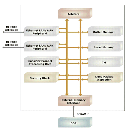
One way to improve both performance and security effectiveness is to reduce the physical number of hardware and software components that make up OSI Layer 2-4 solutions in the network using an integrated silicon based “subsystem” approach. Silicon based communications subsystems such as the one shown below now offer new architecture alternatives that promote faster performance and enhanced security.

The availability of submicron technology now allows these subsystems to be cost effectively manufactured in silicon as integrated Layer 2-4 solutions. However, the cost of designing these devices can be expensive. A silicon approach then further benefits because communications subsystem IP provides the necessary functionality and performance while minimizing the design overhead.
The opportunity to more effectively coordinate network packet management and security using an integrated silicon approach, and the trend towards silicon based subsystem architectures, has led merchant semiconductor intellectual property suppliers to offer communications subsystem IP. The remainder of this white paper will focus on the benefits of a subsystem IP solution approach and solutions available today from Posedge.
The Value of Integrated Packet Management and Security
One simple view of the Internet is that it is a distribution channel for digital packets that are sent to and from many places around the globe. The objective is to deliver these packets as fast as possible to the people who are authorized to receive them. Today, the Internet is built using a massive amount of components that work together to form the distribution channel. An empirical analysis of the support trends for each OSI Layer yields a clear glimpse into why it is getting increasingly difficult to improve both network packet performance and security:
- There are now many physical layer standards that support various transfer rates
- There are many silicon based off-load solutions that address pieces of the network
- There is a myriad of software that must be coordinated with the myriad of silicon/hardware to implement the Layers.
- There is a myriad of applications that have been developed that rely on the resources of the lower layers for achieving the performance and security levels required by the user.
The infrastructure of the channel itself has become a limiting factor to improving performance and security. Achieving interoperability is so complex with so many vendors participating that innovations in some areas produce new design challenges in other areas. Therefore, consolidating OSI Layer support using integrated silicon based architectures streamlines the number of components that make up the network, and creates the opportunities to deliver performance and security improvements while maintaining interoperability.
Advantages and Challenges of Silicon Integration
Offload engines for TCP, IP, IPsec, and for security processing such as certificates, are examples of silicon available from a multitude of vendors that are used to improve performance for an OSI Layer. Semiconductor IP used for these products allows companies to amortize the cost of silicon development across a greater number of applications, which serves to lower the overall cost per product.
However, as requirements continue to grow, most design starts are also targeting multiple adjacent market segments. In some cases, companies do not possess all the expertise required to engineer such a solution. In other cases, these resources are spread far and wide, and it would be a formidable task to centralize them in order to make such a project feasible. So while the integration of multiple Layers is attractive, these projects require vast system integration expertise, as well as the building block IPs. It is this expertise that adds significant expense to the project, because specialization in all Layers requires teams of experts, not just a few individuals.
The Benefits of Merchant Subsystem IP Solutions
Semiconductor communications subsystem IP development costs are amortized across a large number of designs. As a result, these deliver better economics with higher value when compared with developing the same solutions in-house because:
- They include all necessary hardware, firmware, and software
- They create opportunities to deliver measurable system performance increases
- They support flexible sub-components which can be mixed and matched with little re-engineering
- PHYs and Secure PHYs for physical connectivity options
- Layer 2/3 off-load engines that improve performance
- Seamless security for Layer 3/4/5 using engines and software
- They can be deployed with far less system power required
For devices built specifically for networking products, the subsystem IP approach is an economical alternative to in house resource consumption. For devices that require network connectivity and additional functionality, the subsystem IP approach isolates the communications functions and allows rapid integration with minimal communications expertise required. In either case, compelling value is created.
Outsourcing the communications subsystem translates into resources made available to innovate and differentiate further at the system level. Here is where diminishing returns because of underlying network performance and security challenges transforms to increased returns based on advancements in the same.
Posedge Communications IP Subsystem Solutions
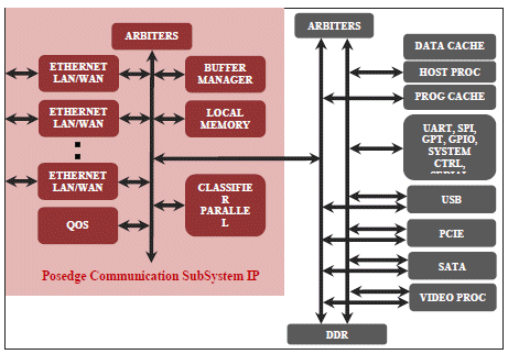
The following is a typical SoC using a Posedge subsystem IP solution:

Posedge solutions routine achieve up to 10 times the performance of conventional approaches. For example, wire speed performance of 64 bytes achieves 2-4 Gps with ultra low area and power. The ability to mix and match functions such as switching and routing, MACsec, IPSec, SSL, and TOE also delivers an unparalleled level of flexibility from one communications architecture. Using this solution, Posedge customers benefit from:
- An integrated packet management and Quality of Service scheme
- Integrated security management at the point of packet management
- Balanced arbitration for optimal off chip DRAM utilization
- Clear partitioning of communications and system domain processing
The “decoupling” of the communications subsystem from other system functions also offers opportunities to make significant changes without re-architecting the entire silicon device. This becomes extremely advantageous for re-purposed silicon across a variety of physical layers, such as Wifi and WiMax. Changing stacks and re-tuning hardware while maintaining consistent architecture significantly lowers the overall development costs.
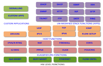
Posedge hardware is complimented with firmware and software (shown below) that enables companies to develop balanced communications subsystems which are flexible to change with minimal re-engineering. This translates to better performance for a given design target, and higher reusability for multiple design targets.

The flexibility of mixing and matching protocols on a programmable hardware IP block further promotes innovation and reuse. Posedge provides for modifications to the standard stacks, and firmware and protocol software that runs on the hardware blocks.
Complete Communications Architecture Analysis Now Possible
An important benefit when using Posedge communications subsystems IP is the availability of comprehensive analysis tools that accelerate the configuration and tuning of the communications subsystem IP. Posedge provides tools for analyzing bus bandwidth, memory, and CPU utilization so that developers can make critical decisions about the operations of the communications subsystem before the actual design start.
As a result, the ability to provide predictable functional and performance modeling in the architecture phase of the silicon design enables system software and chip designers to begin their development tasks more rapidly, and experience less iterations, which translates into faster time to market and lower development costs. This leads to parallelizing hardware and software development timelines, which represents a significant breakthrough for silicon development.
Usher in a New Level of Specification Development
Posedge engineering resources are often viewed as experts for a wide variety of communications applications. As such, including Posedge consulting services as part of the architecture team allows Posedge customers to develop specifications for key requirements while ensuring the resulting silicon device will be the best in class. With expertise in hardware and software, Posedge engineers perform optimal trade-off analysis when partitioning the solution between hardware and software.
Enabling New End Markets
Posedge solutions enable new market segments for customers’ products, thereby increasing the return on investment on the silicon developed. For example, Posedge is currently offering its 10 Gbps MACSec solution to make simple 10 Gbps Ethernet PHYs to Secure PHYs for the Datacenter market. The rich set of expertise that Posedge maintains provides Posedge customers with a turnkey approach. A solution is brought to market economically with little expertise required beyond Posedge consulting services.
Changing Economics Dictates New Approaches
The ever growing need for more and more digital appliances to connect to the Internet, and the constant pressures to lower the cost while improving the performance and security of that connectivity means that the economics of supporting Internet connectivity must change. The emergence of communications subsystem IP offers a highly adaptable low cost way for silicon suppliers and system vendors to provide secure high performance connectivity while lowering both their development and resulting chip costs.
The shift from design instance to architecture that Posedge communications subsystem IP provides enables Internet connectivity implementations to remain consistent across many generations of silicon and system deployments. This serves to lower development costs further as these architectures are used across a wider array of devices with minimal re-engineering. The consolidation of the packet management and security also enables for better analysis and design, and therefore acts as a catalyst for system level innovation, which is most likely where differentiation by the end user will be most valued.
Shifting to a silicon based communications subsystem IP strategy then creates the new economics by which supporting Internet connectivity can be made a profitable endeavor.
Related Semiconductor IP
- Ultra-Low-Power LPDDR3/LPDDR2/DDR3L Combo Subsystem
- 1G BASE-T Ethernet Verification IP
- Network-on-Chip (NoC)
- Microsecond Channel (MSC/MSC-Plus) Controller
- 12-bit, 400 MSPS SAR ADC - TSMC 12nm FFC
Related Articles
- Advancing Network Packet Management for Converged NIC
- Security Chip Design Speeds on to Silicon
- Islands in the power management storm (by Barry Hoberman, President and CEO of Virtual Silicon)
- Power Islands: The Evolving Topology of SoC Power Management
Latest Articles
- Extending and Accelerating Inner Product Masking with Fault Detection via Instruction Set Extension
- ioPUF+: A PUF Based on I/O Pull-Up/Down Resistors for Secret Key Generation in IoT Nodes
- In-Situ Encryption of Single-Transistor Nonvolatile Memories without Density Loss
- David vs. Goliath: Can Small Models Win Big with Agentic AI in Hardware Design?
- RoMe: Row Granularity Access Memory System for Large Language Models