Advanced Techniques for IP Design and Verification
NXP Semiconductors
Bangalore, India
Abstract :
As designs grow in size and complexity, the challenges associated with low power and the growing design and verification gap have created the need for a paradigm shift in the IP design and verification methodology from the traditional approaches. SystemVerilog for design, power aware design and verification flow, dynamic and formal property verification and transaction level debugging for viewing signals at a higher abstraction level are some of the new techniques getting more attention in the design and verification space.
This paper will highlight the benefits of these techniques by using the on-chip interconnect (Network on chip) reference design as case study and the current trends with respect to the EDA industry.
I. Design and Verification challenge
The rapid increase in design complexity due to shrinking semiconductor process technology and greater time to market pressure require improving design productivity and reducing the time to market.
Tapeout delays and frequent re-spins due to late design bugs are the major issues in today’s SoC design world. Several studies have shown that the number of bugs in the RTL is directly related to the number of lines of HDL code. The traditional HDL languages (VHDL/Verilog) do not address these problems. Using HDL language constructs that describe the functionality with reduced lines of HDL code is a key requirement to reduce the bugs in the silicon.
Verification is one of the biggest challenges in the design of modern System on chip and reusable IP blocks. Traditional verification methods do not keep up the ever-increasing size and design complexity. Simulation based dynamic verification approach offers scalability, trying to cover the functional space through constrained random & directed testing. But it also sometimes fails in its objective because of the complexity involved in reaching all scenarios, detailing of complex testcases & the huge simulation runtimes they involve if required covering all the scenarios. On the other hand formal methodology holds the promise of completeness, guaranteeing the quality and closure of verification. But unfortunately it restricts the size & type of the designs that can be handled. With these newer techniques the challenges in verifying reusable and highly configurable complex IP components still persist. The requirement is a methodology to integrate efficiently both these techniques and to speed up the debug process to enhance verification productivity.
II. Advances in Design and Verification methodologies
Fig 1 shows advanced design and verification methodology aided by SystemVerilog based design, SystemVerilog assertions, formal , dynamic verification, CPF based power characterization and transaction based debug
A. SystemVerilog for design
SystemVerilog provides a number of advantages over traditional Verilog/VHDL including improved design specification, code reuse and unified design and verification. Its advanced design constructs yield more compact RTL code, typically a two-to-four times reduction in the RTL lines thereby increasing the design productivity. SystemVerilog achieves improved design specification by allowing related functionality to be described as a single object. Examples of this improved description include bus design using interfaces, data collection using structures/unions and type sharing using packages.
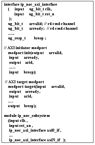
Interfaces in SystemVerilog are designed to model communication between modules keeping the description in one place. Interfaces encapsulate protocol and signals for communication. Using built-in assertions for protocol compliance, the interfaces can be pre-verified. The IP blocks connecting to the interface need to be verified only for functionality and not for wiring between the components. Verifying the interfaces in the chip infrastructure independently reduces the chip level verification complexity to a larger extent.
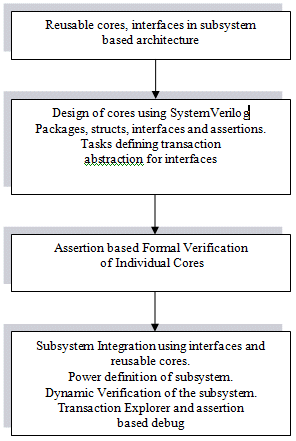
Fig 1: Advanced Functional Design and Verification flow
interfaces can be pre-verified. The IP blocks connecting to the interface need to be verified only for functionality and not for wiring between the components. Verifying the interfaces in the chip infrastructure independently reduces the chip level verification complexity to a larger extent.
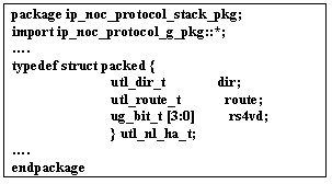
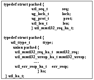
The SystemVerilog struct and union construct allows for modeling user defined structures. The grouped data items in the structure can be treated as a single object, they no longer be defined repeatedly, thereby reducing code size, allowing code reuse and enhancing readability. The following example illustrates the use of structures and unions.
The data collection items and type definitions no longer need to be declared repeatedly, but can instead be defined in a package, reducing the code size, enhancing readability and supporting code reuse.
SystemVerilog constructs allow the designers to express the intent clearly in a way the simulation and synthesis tools can have a unified view of the RTL.
The always_comb construct in SystemVerilog allows the designer to describe the hardware specification for combinational logic. Synthesis tools can check that the hardware synthesized from the block does not contain any flip-flops or latches. In addition, the usage of this construct ensures that simulation will behave closely with the synthesized result.
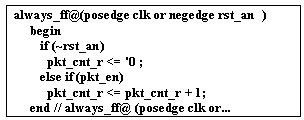
The always_ff block in SystemVerilog ensures that the hardware being described contains a flip-flop.
B. Power aware design and verification
Power management in SoCs require a design flow that integrates power saving technologies to the greatest possible extent. Such a flow should allow us to capture the intent of SoC architects and designers throughout the design cycle. This requires the intent to be captured in a common power specification format that be can used and shared across the entire design flow from architectural specification to the backend layout. CPF (Common power format) is a new power language which captures the power management intent and it enables the automation of low power design techniques. In this paper we will focus on the power awareness in the design and verification flow.
Power awareness in the design flow helps to know the target voltage(s) for the chiplet/subsystem so that the designer can better understand the various area, timing and power requirements for the block. If the SoC supports multiple power islands, level shifters must be inserted between domains and they can have an influence on the timing requirements by adding to the cell delays. The block level micro architecture can be explored taking into account the need for retention registers, different modes of operation, power sequencing, power consumption, area utilization and for performance (Quality of service).
Power aware verification helps to identify the functional and structural problems in the design, major reason for failure in Multi-Vdd SoCs. The structural problems include missing level shifters, missing isolation cells and bad power and grounds connections. The functional problems include illegal state retention or power down/power up sequence. Dynamic and/or formal analysis techniques can be used to identify the power problems in the SoC.
C. Incorporating Formal and Dynamic verification flow
With reusable subcomponents approach it is possible to perform more efficient and productive verification combining both simulation based dynamic and assertions based formal verification. The subcomponents with smaller size and common interfaces are ideal for formal verification which helps to achieve completeness and greater depth in functional space coverage in a quick and efficient manner. The goal for verifying these subcomponents are completeness in verification of the functional space. At the subsystem level requirement in terms of verification are scalability and a time bound closure in coverage of the functional space. Dynamic verification is performed at subsystem level by building reusable, constrained random, coverage driven testbenches.
D. Transaction level debugging
Most designs are modeled at the Register Transfer level for which the simulator will only produce signal-level trace data. With bus based protocols and packet based communication signal level data becomes difficult to track and comprehend. On the other hand if the signal level data can be made automatically available at an abstract transaction level for analysis and visualization a heck of a lot of time can be saved in avoiding manual "reading" of simulator-returned signal values. Transactions provide an abstraction of signal-level activity that is easier to comprehend, analyze, and debug. By moving to transaction level tracing & debug we can realize significant productivity gains by viewing and analyzing this data at a higher level of abstraction.
III. Network on chip – Case study
The network on chip interconnect at NXP caters to the vision of scalability, support for multiple power islands, guaranteed QoS (quality of service), and a configurable interconnect strategy. The design and verification of the various cores, components and subsystem in the Network on chip interconnect is based on the different methodologies discussed above and are applied to reap the maximum benefits.
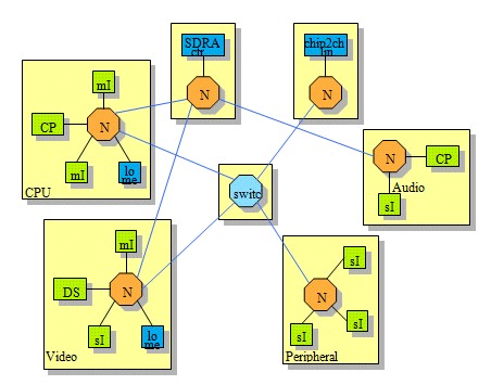
Figure 2 shows the NoC interconnect with network interfaces, switch and end targets.
A. SystemVerilog Packages and Cores
The Network on chip protocol is a packet based communication built on the OSI stack model. The packet headers and payload are defined as structures/unions in SystemVerilog in packages.
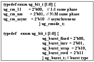
The constants/parameters are defined as enumerated types for improved readability and debugging.
The NoC interconnect internal interfaces are declared seperately and pre-verified with built-in assertions. The monitors for the transaction level debugging are also added part of the interface declaration.
B. Verification
With all the complexity and different requirements IP verification can no longer be a single technique approach. Instead it is an integration of multiple verification techniques carried out precisely so that it is more effective than merely a sum of techniques. We combine both formal and dynamic verification methodologies to increase verification productivity. Since the design is broken into smaller cores and subcomponents which are reused extensively for designing the subsystem we can use formal for verifying them. At the subsystem level these cores are integrated and verified using dynamic simulation.
B.1 Formal Verification
Arbiters are used in the on chip interconnect to implement the Quality of Service requirements. They are reused extensively in different network components in different configurations within the on chip interconnect. This is mainly a control block which is very suitable for formal verification. Various configuration aspect, request grant behavior, control signal features of the arbiter were covered formally. Other than the design features Quality of Service features of the arbiters are also verified formally. Different QoS requirements like hard real time, soft real time and best effort require different assumptions and assertions on the request and grant behavior. Based on these assumptions and assertions written in SVA arbiter performance for different configurations was verified formally.
Within the design we have multiple entry fifos which are used for buffering as well as clock domain crossing. This block with all the properties is verified through formal verification. Also the data ordering for the fifos can be verified formally for a reduced data width dimension since with the actual data width the state space gets exploded and formal does not give a conclusive result. But at the same time reduction in data width does not affect the ordering functionality. With such mechanism we could also verify some of the data path related properties. For the clock domain crossing since vector fifos are involved testing of the gray coding and its behavior for different valid and accept combination was completely verified based on formal.
The on chip interconnect also needs to support standard external interfaces like AXI, AHB, proprietary interfaces like MTL, DTL so that we can hook IPs with these interfaces directly to the on chip interconnect. For supporting this requirement we convert internally all the above protocols to an internal interface protocol. This is done using thin adapters. Since all these protocols are standard interfaces assertions can be written for these protocols which can be used to verify formally the behavior of the thin adapters.
In all formal verification was applied to test the functionality of the arbiters, multiple entry fifos, thin adapters, power management, data link layer and physical layer logic. These modules which are small in size control oriented blocks and reused extensively are the right candidates for formal verification. SVA is used to write all the design and interface assertions and assumptions. Also cover points are written in system verilog to check that all aspects of the design are covered during formal verification. Also the assertions written for these modules are reused as part of the subsystem level verification.
B.2 Dynamic Verification
The only limitation to the formal methodology being used at subsystem level is due to the limited capacity of formal tools, in terms of the sequential depth and size of the design. This leads to unpractical or unpredictable execution time. The subsystem verification is instead based on constrained random, coverage oriented dynamic simulation. An approximation to the problem of the verification is provided by dynamic verification, at least for those properties that are out of the tractable size for formal technology.
Since the entire on chip interconnect is configurable a verification environment is created so as to extract automatically a tailored verification environment for specific on chip interconnect configuration. This involves embedding the design and verification environment in a scripting language and extracting the required configuration. Focus on the system level verification is on reuse which involves reusing the existing verification environments or components of verification environments developed. It includes verification code reuse (monitor, bus-functional model [BFM], scoreboard, data item), and assertion reuse. Since the design has interfaces with multiple instantiations we could create and reuse lot of the verification components for these interfaces. Verification IP or an eVC, a verification component in the e language, was built for these interfaces. It is a ready-to-use, configurable verification module, typically focusing on a specific protocol or architecture. For other standard interfaces like the AHB, AXI, MTL and DTL we used the existing e verification components. Since we are using constrained random verification it is important to know which of design features has been hit. Coverage metric provide this information which helps in gauging verification completion and determine where to focus next if coverage is not sufficient. Functional coverage on the interfaces are part of the verification component. Internal design assertions form part of the design features that need to be covered. Also the assertions written as part of the formal verification can be reused during the dynamic simulation. These assertions are also useful for aiding the debug process when the assertion fails. They help in debugging in terms of taking us closer to the root cause of the issue.
C. Transaction Explorer
To aid the debugging process for all the protocols instead of viewing and tracking the signal level data obtained from the simulator we use tasks to automatically convert all signal level data to transaction level information. These tasks are called at the level where the interfaces are instantiated.
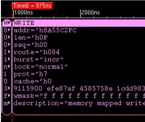
Fig 3: Transaction Explorer.
Tasks use standard APIs provided by the tool vendors. Using these tasks all the signal information for standard interfaces and design specific interfaces can be viewed at transaction level. In case of a packet based communication for the network on chip concept it is complex to track the signals and comprehending the type of the ongoing packet. With additional features like interleaving, signal level information is almost impossible to comprehend. But with a higher abstraction of transactions no effort is required to track the packets as information is reported at transaction level. Also with interleaving supported the interleaved information looks as overlapped transactions on the transaction browser. Transaction-level debug provides the bridge between different abstraction layers and enables advanced bus and network analysis by representing complex signal behavior in a way that can be easily comprehended.
D. Power Definitions
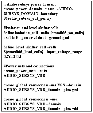
Here is a example for the audio subsystem CPF. The common power format file creates power domains and power nets for the audio subsystem. It also defines the isolation and level shifter cells to be used for communication across power domains.
IV. Conclusion
Using standard industry tools we could design, power characterize, simulate, formally verify and synthesize the system verilog based network on chip interconnect successfully.
SystemVerilog based coding made the code more readable and easily reusable. Also the total lines of code reduced by more than 50 percent.
Break up of the design into smaller cores and subcomponents and formal verification of these components lead to early bug detection and better quality of design components. With formal verification performed on the subcomponents constrained random based dynamic verification could focus on the uncovered functional aspect reducing the overall time for verification closure and a higher confidence on the on chip interconnect.
With transaction based explorer, there is manifold improvement in the debugging process and it no more seems to be a tedious task.
V. References
1) SystemVerilog Language Reference Manual
2) Common Power Format specification
3) Power forward Initaitive
4) IEEE 1647
5) Optimizing Chip Debug through Transaction Extraction with SystemVerilog Assertions
6) Cadence Incisive formal verifier IFV,
Related Semiconductor IP
- NPU IP Core for Mobile
- V-by-One® HS plus Tx/Rx IP
- MSP7-32 MACsec IP core for FPGA or ASIC
- 100G / 200G / 400G / 800G / 1.6T MACsec
- 32 bit RISC-V Multicore Processor with 256-bit VLEN and AMM
Related White Papers
- Formal-based methodology cuts digital design IP verification time
- Plug-n-play UVM Environment for Verification of Interrupts in an IP
- Low Power Analysis and Verification of Super Speed Inter-Chip (SSIC) IP
- Challenges and Benefits of Low Power Design Verification with CPF for a standalone IP
Latest White Papers
- Concealable physical unclonable functions using vertical NAND flash memory
- Ramping Up Open-Source RISC-V Cores: Assessing the Energy Efficiency of Superscalar, Out-of-Order Execution
- Transition Fixes in 3nm Multi-Voltage SoC Design
- CXL Topology-Aware and Expander-Driven Prefetching: Unlocking SSD Performance
- Breaking the Memory Bandwidth Boundary. GDDR7 IP Design Challenges & Solutions