Embedded software development using an interpretive instruction set simulator
Filip Rak, Evatronix, Bielsko-Biala, Poland
Wojciech Sakowski, Institute of Electronics, Silesian University of Technology, Gliwice,Poland
Abstract
This paper presents an instruction set simulator of an 8-bit, MCS-51 compatible CPU core, and shows how to use it in embedded software development process; Method to control and debug CPU using embedded Tcl script interpreter via universal debug interface is also discussed.
Motivation
Technological progress causes complexity of systems-on-a-chip (SoCs) to grow rapidly in last few years. Millions of logic gates and sophisticated analog circuits are usually controlled by the one or more CPU, running an application – very often hundred of thousands lines of source code, that is intended to work under control of operating system. Simulation of such SoC is difficult – apart from hardware part (which is very expensive to simulate in terms of time), there is also need to debug application. There are two standard ways:
- Using native compilation
- Using RTL model of CPU
These methods have drawbacks – native compilation does not give any architecture-dependent details and does not allow to simulate multithreading, while RTL model of CPU introduces overhead from simulating CPU itself.
The solution for these problems is to use instruction-set simulator (ISS); ISS functionally behaves as model CPU, but it does not map any internal architecture and thus – it simulates four to five rows faster, compared to the RTL. Since ISS is intended to control rest of the SoC, it must be equipped with appropriate interfaces to communicate other components. As the solution, recently introduced TLM 2 standard was chosen to be implemented in Evatronix ISS modules.
R8051XC processor core
R8051XC core is a fast version of Intel™ MCS51 CPU, designed at Evatronix company. It is intended to be used in ASIC or FPGA implementations.
Main R8051XC features:
- 8-bit instruction decoder
- Reduced instruction cycle time (up to 12 times, compared to the original MCS51)
- 8-bit arithmetic and logical operations, also 8 x 8 multiplication / division
- External code and data memory bus
- Standard 8051 peripheral set:
- Timer 0 & 1
- Timer 2
- UART
- Interrupt controller
- Configurable set of SAB80C515 peripherals:
- 32-bit multiplication/division unit
- Additional 16-bit timers/counters
- I2C interface unit
- SPI interface unit
- Full duplex serial interface
- Code and data memory banking
- DMA controller
- Built-in On-Chip Debug System
In order to facilitate software development and debugging process, the On-Chip Debug System (OCDS) was incorporated into R8051XC core. It provides set of features for controlling CPU state and accessing its internal resources:
- Application flow control (run / stop / step)
- Internal registers read / write access
- Code / data memory read / write
- Data access breakpoints
- Software breakpoints (by inserting A5 code, which is illegal on standard MCS51 CPU)
R8051XC Instruction Set Simulator (R8051XC_ISS) – overview and model features
R8051XC_ISS is a transactional model of R8051XC in its full configuration, designed using C++ with external SystemC TLM wrappers (using TLM 2 library). Functional conformance with RTL core allows to perform software simulation at high speed, while still providing sufficient detail level to catch application bugs and bottlenecks.
Several assumptions were made for the ISS model:
- Instruction-accurate functionality, no internal micro architecture is modeled
- Pure C++ language using only generic types to improve simulation speed
- Set of TLM wrappers to use ISS in SystemC environment
- Static design with no internal processes
- Look-up table instruction decoder, optimized for high-speed opcode processing
- Either no time dependencies (pure PV model), or annotated timing (PV+T) with instruction-level time granularity
- Standard communication interfaces (like TLM 2 for accessing external memories)
Architecture description
Base configuration of ISS model consists of eight main parts, as shown on figure 1 (for TLM 2.0 wrapper there are CODE and XDATA memory sockets that use tlm_generic_payload, instead of sc_ports).
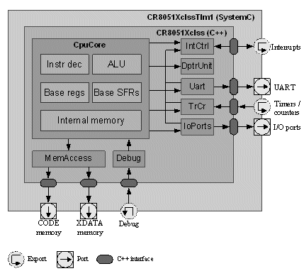
Fig. 1 Architecture of R8051XC_ISS
Main CPU functionality, which includes instruction processing unit and internal data (memory and registers) storage is placed in CpuCore. Together with memory access module, they implement all features needed to process the application:
- Fetching instructions from the CODE memory
- Decoding opcodes and calling appropriate processing routine
- Processing incoming interrupt requests
- Providing access to internal data memory and SFR space
- Handling basic statistics (number of instructions processed etc.)
Since R8051XC in its full configuration allows to address up to 8 MB of CODE space, the PC register is implemented as unsigned long value with variable bit mask, regarding on actual address bus width.
External code and data memory is accessed via MemAccess unit – it provides unified memory port, that is independent of external interfaces (pure C++, TLM 1.0 or TLM 2.0). This sub-module also implements data access breakpoints. List of features:
- Unified external memory port
- Data access breakpoints
- Optimized for external interface
Two described sub-modules – CpuCore and MemAccess are the main parts of an ISS. The remaining five implement MCS51-compatible peripherals.
Incoming interrupt requests are processed by the IntCtrl unit. It contains priority resolving logic, together with interrupt masking functionality. In case the interrupt is accepted, information is passed to the CpuCore and appropriate routine is being called. Features:
- Interrupt masking
- Priority handling
Since TLM library does not provide standard interface for requesting interrupts, R8051XC_ISS uses tlm_transport_if bidirectional interface to support interrupt handling (requesting and providing status – accepted / rejected).
Data pointer (DPTR) register has its own sub-module, DptrUnit. Since DptrUnit functionality would vary, depending on configuration, there are three implementation. Base features summary:
- DPTR byte and word access
- DPTR incrementation
These features are supported by the basic DptrUnit module. The second one allows to use two DPTR registers (handled via four separate SFRs and DPTR selection bit), while the last implementation supports eight DPTR registers with arithmetic:
- DPTR auto incrementation / decrementation
- DPTR cycling
UART sub-module implements serial unit, present in 8051 CPU. It provides four transmission modes – both synchronous and asynchronous. allows to transfer byte data through two signal lines. Features:
- Four transmission modes
- Selectable baud rate for asynchronous transmission
Full configuration provides also second UART unit, that allows full-duplex operation.
Two timers and counters (T0 and T1) are implemented in TrCr sub-module. Features:
- Full T0 and T1 functionality
- Interface for counting external events
The last sub-module, Debug, implements whole functionality related to flow control and accessing CPU internal resources. It implements set of operations defined in debug_if class, which is common for ISS components made in Evatronix. Features:
- ISS initialization and reset
- Flow control (running / stopping / making one or several steps)
- Bi-directional (read / write) register access
- Internal and external memory access
- Data / execution breakpoints
- Interrupts triggering
As mentioned above, ISS is designed in C++ (without using SystemC modules), just to allow integration into custom debug DLLs (for example, into Keil uVision™). External communication is done by means of pointers to interface classes. In order to be able to integrate component into SystemC environment, the TLM wrappers were designed:
- One using tlm_transport_if interface with template request and response structures; communication is done via ports
- Another using tlm_generic_payload and TLM 2 sockets
Both wrappers are optimized to gain high simulation speed.
Architecture details
Instruction decoder
Instruction decoder in R8051XC_ISS is designed to use look-up table (LUT) , to gain high, constant decoding time. Such a table holds instruction descriptors that describe:
- Instruction kind (enumeration)
- Number of instruction bytes
- Pointer to the processing method
- Extra instruction data
Since each MCS51 instruction can be identified uniquely by reading only its first byte, LUT may have 256 entries and is relatively simple. Decoding schematic:
- Single instruction byte is read from address pointed by the PC register
- Read byte is used to index LUT and to get instruction descriptor
- Using number of instruction bytes from the descriptor, all remaining bytes are read from CODE memory
- Member pointer (also from the descriptor) is used to call appropriate processing method
External memory access
After introducing TLM 2.0 standard, appropriate wrapper was designed to allow fast integration with components that use new standard.
Memory exchange bus concept in TLM 2.0 relies on tlm_generic_payload and sockets, which are port/export pairs to support forward and backward data exchange path. ISS communicates with external memories through MemAccess module and through external wrapper – so there was need to make new MemAccess implementation. Generic memory read / write methods were rewritten to:
- compose tlm_generic_payload object
- send the object through external socket (available via reference)
- read and parse result
Data access breakpoints
Data breakpoints are main tool used in software verification process. Since main memory access interface in R8051XC_ISS is TLM 2 generic payload, breakpoint logic can be unified and shared among other projects that need such functionality. There are three kinds of breakpoints supported:
- Read
- Write
- Instruction fetch
Each of these have configurable trigger conditions regarding:
- Address range (or address mask)
- Data range (or data mask)
Internally, breakpoints are stored in two arrays – first keeps all breakpoints, regardless their state (enabled / disabled); second one holds only active breakpoints and is used to speed up access tracking. Steps taken when memory access request arrived:
- Operation type is checked (e.g. read accesses do not trigger write-only breakpoints)
- Address is validated against breakpoint conditions (either range or value/mask)
- If data tracking is enabled, then appropriate condition is checked (either data range or value/mask)
Algorithm overview is shown on figure 2.
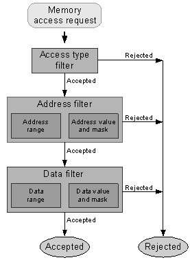
Fig. 2 Data breakpoint algorithm overview
External SFR interface
In case of MCS51, only few SFRs are related to CPU core functionality; most belong to the peripheral modules. Since R8051XC is configurable, there is need to provide fast and flexible mechanism for connecting additional modules and mapping their SFRs. R8051SC_ISS uses delegate approach: SFR read / write delegates are stored in two arrays (one for read and the other for write ones), which are indexed by the SFR address; if there is no delegate (corresponding pointer in the array is equal to NULL), then access is directed to the external SFR interface.
Testing environment
Overview
R8051XC_ISS was fully verified using co-simulation with Verilog RTL model. After loading the same application (from external HEX file), program was executed step by step. After each step, CPU state (registers and internal memory contents) were compared – each difference was considered as error and stored in log. RTL model was wrapped in TLM2-RTL transactors and debug interface is provided by JTAG interface, using appropriate library. Test is driven by Tcl script console with mapped debug commands. Figure 3 shows schematic of verification environment.
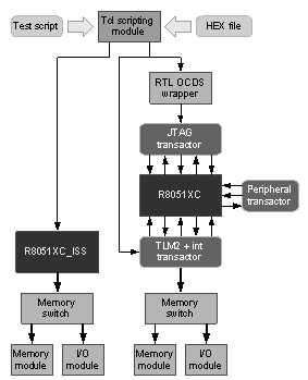
Fig. 3 Testing environment schematic
Tcl console
debug_if interface class is common for ISS models designed by Evatronix. Besides debug functionality, it allows to enumerate CPU resources such as:
- Basic CPU parameters
- internal registers
- memory interfaces
Direct usage of debug_if interface is not convenient – user must write testbench-like module for particular application, which is not flexible and time consuming. To ease debugging task, binding module for Tcl scripting language was developed. Tcl interpreter is wrapped with class and equipped in easy-to-use function / method registration routines (using template-based delegates); debug_if interface methods were mapped to appropriate Tcl functions, that can be called directly in Tcl script, which allows to take advantage of powerful scripting engine. R8051XC_ISS package includes also simple Tcl console, which allows to write debugger scripts “by hand” or reading them from disk files. Due to easy extensibility, Tcl syntax can be enriched with other functionality, as needed. Features:
- Object-oriented interpreter wrapper
- Delegate-based Tcl routines mapping to methods / functions, using automatic and type-safe parameter conversion
- Built-in HEX file parser and writer
OCDS functionality
R8051XC_ISS is equipped with unified debug interface, that allows to control CPU. In some cases (e.g. integration with external debuggers), there is need to have exactly the same functionality as one in RTL model – it is done by the OCDS sub-module, which is a bridge between Nexus™ compatible register architecture and debug_if method calls. Moreover, built-in TAP FSM and JTAG™ slave interface is able to interact with JTAG signals (tck, tms, tdi, tdo, trst) and to translate sequences into NEXUS registers read / write accesses. Both interfaces are also available from Tcl script level.
Simplified OCDS architecture is shown on figure 4.

Fig. 4 OCDS architecture
Interfacing ISS with the TLM model
Simple system was developed to prove ISS usefulness in software development process. R8051XC_ISS is interfaced with USB-OTG model, using developed TLM2-RTL AMBA AHB™ transactors. On the other hand, the same system with R8051XC component was designed. Both CPUs were running the same application that consists of software stack and simple transmission code. Figures 3 and 4 show overview of both systems (with ISS and CPU RTL model, respectively).
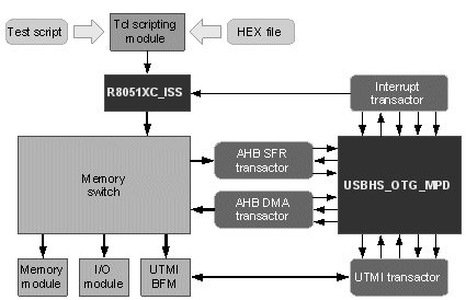
Fig. 5 USB system-on-chip using ISS component
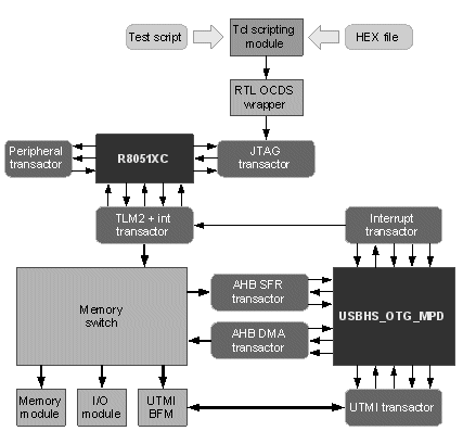
Fig. 6 USB system-on-chip using ISS component
Application
Application that uses software stack to interface with USB model (as well RTL as TLM one) tries to communicate with other devices on the USB bus (USB bus “logic” is enclosed in UTMI BFM component, that is configured and controlled from the application via SFR interface). As in case of real device, firstly enumeration is made (CONTROL transmissions using endpoint #0), then bulk transmission is performed (some random block accesses), and – at the end – isochronous transfers are launched.
Conclusions
Intruduction of ISS into SoC design flow radically simplifies embedded software development and verification process. Simulation speed reaches 8 million instructions per second (without taking SystemC kernel task switching under consideration), which is sufficient for testing purposes and is few rows larger than in case of RTL model. Project also proved possibility of easy replacement RTL model with its TLM-based equivalent with no significant differences in functionality. Furthermore, when using JTAG pin OCDS interface (present in R8051XC_ISS) it is possible to connect Tcl scripting console (via JTAG transactor) with real hardware (implemented in ASIC or FPGA) with little effort – in such case some of debug features (e.g. interrupt requesting) are not available, but still software can be debugged using standard debugging routines set.
Software special features (like dynamically loaded, self-modifying code, even working under RTOS control) can also be handled thanks to interpretive architecture of R8051XC_ISS (it processes application code instruction-by-instruction) (interpretive ISS). PVT mode (implemented as wait() calls and per-instruction cycle computation) allows to identify possible bottlenecks and to estimate performance margin in time-critical applications. Tcl debug console allows to perform long, automatic tests by taking advantage of powerful scripting engine.
Literature
1. R8051XC Design Specification, © Evatronix SA, 2006
2. USBHS-OTG-MPD Hi-Speed On-The-Go Controller for Multiple Peripheral Devices Core Specification, © Evatronix SA, 2006
3. SystemC: From the Ground Up, David C. Black, Jack Donovan, Kluwer Academic Publishers, 2004
Related Semiconductor IP
- NPU IP Core for Mobile
- NPU IP Core for Edge
- Specialized Video Processing NPU IP
- HYPERBUS™ Memory Controller
- AV1 Video Encoder IP
Related White Papers
- Development and use of an Instruction Set Simulator of 68000-compatible processor core
- Dynamic instruction set load-in method for Java SoC
- Design of a 8051 Microcontroller in FPGA with reconfigurable instruction set
- Extending RISC-V ISA With a Custom Instruction Set Extension
Latest White Papers
- Breaking the Memory Bandwidth Boundary. GDDR7 IP Design Challenges & Solutions
- Automating NoC Design to Tackle Rising SoC Complexity
- Memory Prefetching Evaluation of Scientific Applications on a Modern HPC Arm-Based Processor
- Nine Compelling Reasons Why Menta eFPGA Is Essential for Achieving True Crypto Agility in Your ASIC or SoC
- CSR Management: Life Beyond Spreadsheets