Internal JTAG - A cutting-edge solution for embedded instrument testing in SoC: Part 2
By Medha Thakar, eInfochips, an Arrow company
In the previous part – Part 1 of this article, we have discussed the shortcomings of JTAG 1149.1/1500 standards to overcome the increasing test challenges accounted for, in the new era of humongous size of ASIC architecture. We also highlighted the significance of IJTAG briefly.
Although there are several papers and architecture describing IJTAG details, we are trying to describe the detailed architecture of IJTAG network interface and its implementation in Part 2 of this article. In this part, we will describe the detailed architecture of IJTAG network interface and its implementation.
IJTAG Network Interface
IEEE P1687 standard of IJTAG comprises of three main components as listed below:
- IJTAG Network Architecture
- Instrument Connectivity Language – ICL
- Procedural Description Language – PDL
1. IJTAG Network Architecture
Under this component, standards provide information on how we do IJTAG network architecture insertion in the test strategy. It has the following components:
Segment Interconnect bit (SIB): As the name suggests, it is a single bit cell that can ‘segment’ the scan path according to the user requirement and the instrument that is to be kept as a part of the active scan path.
It acts as a door or a switch. When the switch (SIB bit) is OPEN, it allows adding the scan path to the IJTAG network. And, when the switch is CLOSE, it would exclude the particular scan path from the network.
When the bit is set to 0, it acts like a bypass register that simply bypasses the instrument. And, when it is set to 1, it includes the instrument on the active scan path.
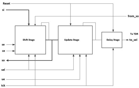
The structure of SIB is described in Fig. 1 below:

Fig. 1 SIB structure [4]
- The input ports are reset, selection signal (sel), capture enable (ce), update enable (ue), shift enable (se), scan input from TAP TDI (si), scan out from TDR (from_so) & tck.
- The output ports are scan out (so) & selection signal for TDR (to_sel).
- SIB generates the local selection signal ‘to_sel’ for TDR.
The signals mentioned here have been given general notations. These are not universal. It varies from tool to tool. The structure may also vary depending on the tool. It has two mandatory stages of shift and update and an optional delay stage. It has two configurations as described below:
- Bypass Register Configuration: When the sel signal is ‘0’, SIB is configured as bypass register. It is shows as the highlighted path in Fig. 1. Path from ‘si’ to ‘so’ to be activated so, it excludes the instrument and the TDR from scan path.
- Activate Scan Path Configuration: When the sel is ‘1’, si value is latched into the shift stage and latched into the update stage at the negative edge of IJTAG Clock. Delay stage is added to avoid any race condition in case TCK skewed between SIB and TDR [4].
Test Data Register (TDR): The access network consists of Test Data Register (TDR), which is similar to, but not the same as those found in JTAG Boundary Scan Standard. TDR has data input ports, si, to_sel, ue, ce, se, tck and data output ports, from_so as its output ports.
2. ICL - Instrument Connectivity Language-
ICL describes the connectivity of the various on-chip IJTAG Network Architecture components with the instruments present on the scan path. It also describes the hardware of TDRs and SIBs present on the chip. The connection of various scan paths with TAP controller is also included. Additionally, it also describes all the active scan path present in the network.
3. PDL - Procedural Description Language-
PDL is a command language that instructs the instrument on how to generate patterns; it is not a pattern description language in itself. The standard documents the representation of test vectors and operations for direct access to embedded instrument. It creates portable test vector, which can be used with the embedded instrument, irrespective of the hierarchy in which it is instantiated. This makes test vector re-usable, not having to go through the tedious task of pattern generation if the instrument has to be embedded at different level of hierarchy. This process of translating instrument level PDL pattern into stimulus at top-level PI and PO is called PDL retargeting [4]. When the top ICL level is reached, PDL may be translated into pattern format [4].
Illustrative example - ICL and PDL Description

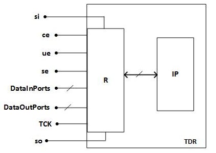
Fig. 2: TDR instance of IJTAG network interface [4]
Every Network component of the IJTAG standard and every instrument have their corresponding ICL description. Consider the IP given in Fig. 2. The ICL description of TDR that controls its instrument can be described as follows:
Module TDR {
ScanInPort si;
ScanOutPort so; {Source R[0] ; }
ShiftEnPort se;
CaptureEnPort ce;
UpdateEnPort ue;
SelectPort sel;
TCKPort TCK;
ScanRegister R[7:0] {
ScanInSource si
}
}
Keywords: ScanInPort, ScanOutPort, ShiftEnPort, CaptureEnPort, UpdateEnPort, SelectPort, TCKPort, ScanRegister
Names of ports: si, so, se, ce, ue, sel, TCK, R
Name of Module: TDR
It is an 8 –bit TDR. The so is connected to the bit 0 of tdr. Hence the source of ScanOut Port is defined as R[0].
PDL description of TDR can be given as:
iProcsForModule TDR
iProc write_to_tdr { value } {
iWrite R $value
iApply
}
iProc run_testX { } {
iCall write_to_tdr 0b10010110
iRunLoop 1000 –tck
iRead R 0xff
iApply
}
All the binding instructions of this PDL are applicable to the TDR module as well as its instantiations.
Keyword ‘iProcsforModule’ identifies that this PDL is for ICL instrument ‘TDR’. PDL is not a pattern description language like STIL/WGL, but it just informs how to generate patterns by writing/reading “care bits” only. Here ‘write_to_tdr’ is a procedure that has a parameter ‘value’ passed. This variable value is used with “iRead” while writing in register ‘R’ $value. ‘iRunLoop’ defines the loop count as 1000 in this case.
This is all we need to do as a user in PDL. We say we want a certain value in ‘R’, the how part is taken care by the tool. We do not write any control signals, all these control signals are taken by PDL.
PDL Retarget
The combined feature of ICL & PDL ensure portability of embedded instrument including its test vectors. In order to retarget the care-bits written for TDR at SoC level, the PDL instruction for SoC will include it in the following manner:
iProcsforModule SoC1 {
…………..
iWrite SoC1.Block1.TDR.R[7:0] 0b10010110
… …
}
As a user, all we do is define the care bits at top-level. The implementation part is taken by IJTAG tool. This is in contrast to the boundary scan, which would require pattern set to be re-written at higher hierarchy where the instrument is instantiated.
The three main features and benefits of IJTAG Standard described in this article can be summarized as:
- Reconfigurable Scan Path – Plug & Play feature of IJTAG
- TDR Organization –Reduced Access Time
- PDL Retargeting – Facilitates system/board level test
Conclusion
Embedded instrumentation is resulting in complex SoC design. IJTAG provides an efficient DFT technique to test them. As discussed in this article, the perfect blend of IJTAG network architecture, ICL and PDL Retarget administer powerful features of plug & play, instrument and test portability to the IEEE P1686 Standard. Moreover, active scan path management decreases test access time.
Author
 | Medha Thakar is working as an Engineer in the DFT BU, ASIC division, at eInfochips, an Arrow company. She has more than 1.5 years of experience in Design for Testing, which includes working on 16nm and 7nm technology nodes, handling block-level, and top-level DFT activities. |
References:
- A Presentation Based on Slides Created by Members of the IEEE P1687 (IJTAG) Working Group, “IEEE P1687 (IJTAG) Draft Standard for Access and Control of Instrumentation Embedded Within a Semiconductor Device” , Jun 2006
- Laung-Terng Wang. Charles E. Stroud. Nur A. Touba, Laung-Terng Wang, “System-on-chip Test Architectures: Nanometer Design for Testability” Morgan Kaufmann Publishers, Version 2008.
- Al Crouch, “IEEE P1687 Internal JTAG (IJTAG) taps into embedded instrumentation” Asset White Paper, Version 2011
- “Tessent IJTAG User’s Manual”, Mentor Graphics Version 2018.1
Related Semiconductor IP
- ReRAM NVM in DB HiTek 130nm BCD
- UFS 5.0 Host Controller IP
- PDM Receiver/PDM-to-PCM Converter
- Voltage and Temperature Sensor with integrated ADC - GlobalFoundries® 22FDX®
- 8MHz / 40MHz Pierce Oscillator - X-FAB XT018-0.18µm
Related Articles
- Internal JTAG - A cutting-edge solution for embedded instrument testing in SoC: Part 1
- Basilisk: A 34 mm2 End-to-End Open-Source 64-bit Linux-Capable RISC-V SoC in 130nm BiCMOS
- FeNN-DMA: A RISC-V SoC for SNN acceleration
- A 0.32 mm² 100 Mb/s 223 mW ASIC in 22FDX for Joint Jammer Mitigation, Channel Estimation, and SIMO Data Detection
Latest Articles
- Quantifying Uncertainty in FMEDA Safety Metrics: An Error Propagation Approach for Enhanced ASIC Verification
- SoK: From Silicon to Netlist and Beyond Two Decades of Hardware Reverse Engineering Research
- An FPGA-Based SoC Architecture with a RISC-V Controller for Energy-Efficient Temporal-Coding Spiking Neural Networks
- Enabling RISC-V Vector Code Generation in MLIR through Custom xDSL Lowerings
- A Scalable Open-Source QEC System with Sub-Microsecond Decoding-Feedback Latency