Interface Timing Challenges and Solutions at Block Level
Interface Timing Challenges and Solutions at Block Level
By Manish Kumar Sagarvanshi (Technical Lead), Madhav Shah (Technical Lead)
eInfochips - An Arrow Company
Abstract
Timing closure of a semiconductor chip is the primary concern for any physical design engineer. Interface timing of a block is as critical as the internal timing. In this article, we will address the challenges faced while fixing the interface timing and the solutions to overcome these challenges. We have used Cadence Innovus as our PnR and Synopsys Primetime as our Sign-off timing tool.
Keywords: IO timing (Input & Output timing), WNS(Worst Negative Slack), TNS(Total Negative Slack), FEP(Failing End Point), ns(nano-second), ps(pico-second), PT(Prime Time).
Introduction
Internal - Clk2Clk timing is always a priority for block-owners working on blocks as compared to the interface timing. A chip-level STA person will always put more margins for interface timing at block-level in the form of higher external delay or higher uncertainties than desired during the timing budgeting. Hence, block-owners do not have to put much effort to converge interface timing.
When there is a requirement of fixing IO timing at the block level, and the top-level does not want to go on cycles of feedback and fixes, in such cases the top-level STA person will provide specific requirements to meet IO timing at early stage of PnR. Following are the general requirement the STA person provides:
- The input and output clock insertion delay requirement, for timing-critical categories of ports in the design
- The skew requirements between ports
- Different types of boundary buffers for different values of loads & critical signals
IO Timing Challenges at Block Level
There are many challenges in meeting the timing requirements at block-level, let's look at four major challenges:
- IO timing miscorrelation at PnR tool (Innovus in our case) and sign-off timing tool (Primetime in our case)
- IO timing miscorrelation at the block level and the top-level
- Flops placement inside blocks, such that optimization buffer/inverter count can be reduced
- Clock-insertion delay requirements
1- IO Timing Miscorrelation between PnR Tool and Sign-Off Timing Tool:
When we take routed design from PnR to Signoff for timing analysis, due to different EDA tool vendors the IO timing miscorrelation may occur.
Following are few reasons for tool-miscorrelation:
- Different uncertainties/margin at PnR and Signoff
- Different extraction engine at PnR and Signoff
- Mismatch in source Insertion delay at PnR and signoff
At PnR, Innovus calculates source insertion delay by taking the mean value of worst corner’s latencies and then apply the same to all the corners. PT does not take source insertion delay from incoming PnR sdc but calculates it separately for each corner. Since PT calculates source insertion delay independently for each corner using StarRC extraction engine, it is more accurate than PnR tool.
For example:
As shown in Table 1, Innovus will calculate mean source-insertion delay value for virtual_clock_1 in the worst corner (FUNC_m40_SETUP_SS_C_WC in our case), that is 0.379ns and then applies the same to all the setup corners.
While in the case of PT, the source-insertion delay value of each corner is different.
| Clock name | Corner name | Innovus Source Insertion delay | PT Source Insertion delay |
| virtual_clock_1 | FUNC_125_SETUP_SS_RC_WC | 0.379 | 0.358 |
| FUNC_m40_SETUP_SS_C_WC | 0.379 | 0.388 | |
| FUNC_125_HOLD_FF_RC_BC | 0.194 | 0.212 | |
| FUNC_m40_HOLD_FF_C_BC | 0.194 | 0.174 | |
| virtual_clock_2 | FUNC_125_SETUP_SS_RC_WC | 0.367 | 0.377 |
| FUNC_m40_SETUP_SS_C_WC | 0.367 | 0.404 | |
| FUNC_125_HOLD_FF_RC_BC | 0.185 | 0.227 | |
| FUNC_m40_HOLD_FF_C_BC | 0.185 | 0.188 |
Table 1: Source-Insertion delay for Innovus and PT
2- IO Timing Miscorrelation between Block Level and Top-Level
There are a couple of reasons, which lead to miscorrelation between block-level and top level IO timing:
- Inappropriate modelling of the driver pin and output load for the IO pins
- Missing constraints
Block constraints like false paths, multicycle paths, external delays, etc. if not appropriately provided in the top-level run or vice-versa can result in huge miscorrelation from block to top-level timing. Few of the other reasons for IO timing miscorrelations are
- Different StarRc and signoff tool recipe or version used at the block level and top-level
- Mismatch in de-rating numbers in the block level and top-level runs
3- Flops Placement near IO ports
During timing optimization, tool will place the flops based on its internal and external timing requirements. Often we have more priority to Internal (Reg2Reg) timing, so flops would be placed a bit far away from the IO ports.
To meet IO timing requirement, we can pull these flops near to respected IO ports but it may impact our internal timing too. Thus, this becomes complex process if such thing happens.
4- Latency requirements
We can have specific latency requirements for IO ports to achieve IO timing at the block level. There are a few challenges we face while achieving these latency targets, like
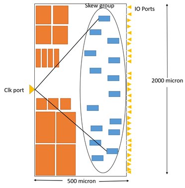
- If the same skew group flops sit very far from each other (as per figure 1) or
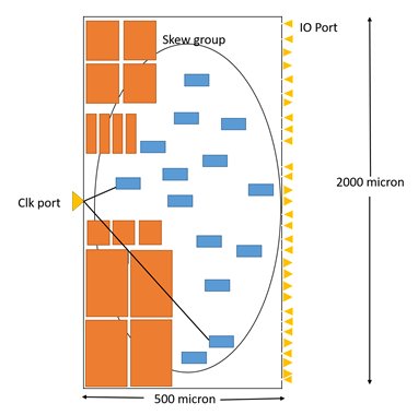
- If the same skew group flops are placed far away from the block-clock port (as per figure 2)
The meeting skew between these two flops affects target latency.

fig 1

fig 2
It is challenging to target lower latency for output ports in a more extended block due to more distance between the flop and port. As we can see in the above figures, clk port to flop distance is around 1000 micron, with this much distance the lower latency is unlikely to achieve.
IO Timing Solutions
There can be multiple approaches to address IO timing challenges. Let’s discuss a few of them:
1- IO Flop Bound at Placement Stage
It is a fundamental and common approach to fix IO timing. In this approach, we need to identify the violated IO ports and make a flop bound nearby to ports. The distance between the port and the flop bound solely depends on the value of IO violation. This approach will help in reducing the number of optimization buffers/inverters in the IO path. Make sure that the bound should not affect internal timing.
Innovus commands for creating bound of the cells:
CreateInstGroup <grp_name> -<grp_type> <bbox>addInstToInstGroup <grp_name> <inst>
2- Insertion Delay Settings at Clock Stage
It is one of the sophisticated approaches to solve IO timing. In this approach, we need to work on the ideal clock insertion delay for violated input and output ports registers.
Let's discuss some essential characteristic of a clock network before digging more into how the insertion delay can help in timing.
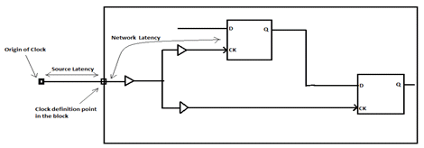
The latency consists of the following components as shown in Image 3:
- Latency: It is the amount of time a clock signal takes to propagate from the original clock source to the sequential elements in the design.
- Source latency: It is the delay from the clock source to the clock definition pin in the design.
- Network latency: It is the delay from the clock definition point to the register clock pin.

fig 3
By default, the tool puts all the clock sinks, driven by the same clock, into a common skew group and balances this with global latency target. Thus, clock insertion delay is effectively determined by the longest sink’s insertion delay.
To address the IO fixing, we need to either pull or push the violated sinks such that it does not affect the subsequent timing path.
We have tried a similar approach in our design with below-mentioned innovus ccopt specific command. It helped us solve IO timing, and we were able to achieve the ideal clock network delay as mentioned in table 2.
For pulling clock by 100ps,
set_ccopt_property insertion_delay 0.10 -delay_corner $worst_corner -pin ${reg_name}/phi
For pushing clock by 150ps,
Set_ccopt_property insertion_delay -0.15 -delay_corner $worst_corner -pin {reg_name}/phi
While pushing tool try to add and for pulling reduces clock buf/inv in the clock path.
| Ports direction | Ports | Default Run latency | Modified Run latency |
| Input | iports1_* | 0.409 | 0.549 |
| iports2_* | 0.420 | 0.560 | |
| Output | oports1_* | 0.471 | 0.369 |
| oports2_* | 0.490 | 0.385 |
Table 2: Ideal Clock Insertion Delay Experiment
| Setup mode | Default Reg2Reg | Default In2Reg | Default Reg2Out | Reg2Reg After clock-insertion delay setting | In2Reg After clock-insertion delay setting | Reg2Out After clock-insertion delay setting |
| WNS(ns) | -0.04 | -0.214 | -0.155 | -0.045 | -0.072 | -0.061 |
| TSN(ns) | -2.255 | -55.47 | -36.268 | -2.381 | -3.61 | -2.782 |
| FEP | 138 | 3895 | 1025 | 145 | 114 | 78 |
Table 3: Timing-Summary
As shown in Table 3, we were able to fix IO timing with this approach, and also made sure that it’s not affecting the internal timing.
It is not always necessary that we will get the desired network delay value as per our settings due to various challenges, which we have discussed earlier. In such cases, we have to try with different insertion delay numbers.
There is a chance of new internal timing violations because of IO flops’ latency change. For this type of scenario, we can enable useful-skew with the following set of commands at the placement stage.
Note- The latency values in these commands will be inverted relative to the set_ccopt_property specification. Therefore, if you want to pull up a pin, the value of CTS insertion_delay should be positive (0.10ns in our case) and set_clock_latency value at placement stage should be negative (-0.10ns in our case).
For Input ports:
set_clock_latency 0.150 {reg_name}/phi
For Output ports:
set_clock_latency -0.10 {reg_name}/phi
There is one more way to achieve IO latency if direct pull/push does not work.
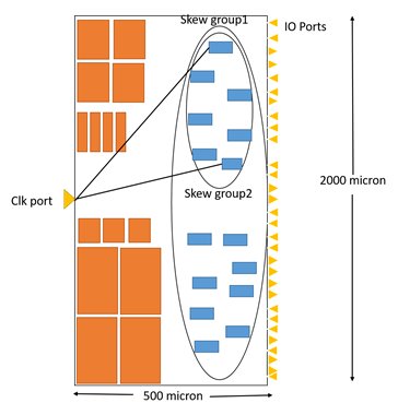
- Create a dedicated skew group for sinks, which have specific latency requirement.
- Specify all these sinks, as exclusive sinks and then specify target latency. The exclusive skew groups always have an exclusive_sinks_rank value greater than zero.
- Once an exclusive skew group is created, CCOpt assigns that exclusive skew group a rank one greater than the highest existing skew group.
create_ccopt_skew_group -name Skewgroup1 -constrains ccopt -source clk -shared_sinks [get_ccopt_clock_tree_sinks $reg_name/clk]
create_ccopt_skew_group -name skewgroup2 -constraints ccopt -source clk -exclusive_sinks {get_ccopt_clock_tree_sinks $reg_name2/clk}

set_ccopt_property target_insertion_delay -skew_group skewgroup2 550
fig 4: Exclusive Skew Group
- After running the first command, a single skew group Skewgroup1 is created. This is a shared skew group, has an exclusive_sinks_rank value of zero. All the "clk" pins in the design are the members as well as the active sinks of this skew group.
- The second command defines an exclusive skew group Skewgroup2. It has given an exclusive_sinks_rank value of 1, which is one higher than the current highest rank of 0.
- Sinks that match the pattern reg_name2/phi are now members of both skewgroup1 and SkewGroup2 but they are only active sinks in Skewgroup2.
- If we are checking input and output port latency through report_timing at block-level then ensure to take care below points.
At top-level, Input port’s register clock pin will be considered in “Capture” path and Output port’s register clock pin will be considered in “Launch” path
For Input ports:
get_property $timingPath capturing_clock_latency
For Output ports:
get_property $timingPath launching_clock_latency
There are few more approaches that can be used for remaining minor IO timing violations such as:
- Net delay improvement: go to the higher layer or ndr
- Swap cells to lowest vt available, increase the drive strength, improve the crosstalk and useful skew at signoff
- Ensure that big-drive strength buffers/inverters are also listed in the clock specification file. Limited buffer list may also cause a problem while building clock-tree
- Routing layer assignment may impact latency due to different RC characteristics. Use non-default rule and multi-cut vias for routing or choose higher routing layers that have smaller RCs
Conclusion
There can be multiple reasons for IO timing violations and therefore you should select the appropriate approach based on the scenario. The solutions provided in this article can help designer to understand interface timing associated challenges and solutions. To simplify IO timing closure not all solutions are applicable to a particular design, but a mix of these solutions can helps the design team to achieve desired results.
References:
- Article (20159220) Title: How to pull up/down the latency to sinks using CCOpt
- Cadence Support Home
Authors:
Madhav Shah has almost 7 years of experience in ASIC Physical Design domain. He holds an Engineering degress in ECE and has worked on various technology nodes such as 28nm, 12nm, and 7nm in Networking SoC and has successfully taped out ASIC chips from RTL netlist to GDS including Sign off process.
Manish Sagarvanshi has more than 5 years of
experience in ASIC Physical Design domain and has more than 1 year
of experience as a Cadence Innovus Application Engineer.
He has worked on various technology nodes such as 16nm
,14nm, and 7nm in Networking SoC and Qualcomm
processor LPF and has successfully taped out ASIC chips from
RTL netlist to GDS including Sign off process.
Related Semiconductor IP
- NPU IP Core for Mobile
- NPU IP Core for Edge
- Specialized Video Processing NPU IP
- HYPERBUS™ Memory Controller
- AV1 Video Encoder IP
Related White Papers
- FPGA prototyping of complex SoCs: Partitioning and Timing Closure Challenges with Solutions
- I2C Interface Timing Specifications and Constraints
- IP Verification : Building systems at the silicon level: time, cost, design constraints
- RapidIO fabric is validated at system level
Latest White Papers
- Breaking the Memory Bandwidth Boundary. GDDR7 IP Design Challenges & Solutions
- Automating NoC Design to Tackle Rising SoC Complexity
- Memory Prefetching Evaluation of Scientific Applications on a Modern HPC Arm-Based Processor
- Nine Compelling Reasons Why Menta eFPGA Is Essential for Achieving True Crypto Agility in Your ASIC or SoC
- CSR Management: Life Beyond Spreadsheets