Improving Battery-Powered Device Operation Time Thanks To Power Efficient Sleep Mode
By Sebastien Genevey, Christian Dominguez (Dolphin Integration)
Allowing battery-powered devices to run, without battery recharge, for years rather than months, partakes in enhancing significantly end-user satisfaction and is a key point to enabling the emergence of IoT applications. Numerous applications, such as M2M, BLE, Zigbee…, have an activity rate (duty cycle) such that the power consumption in sleep mode dominates the overall current drawn by the SoC (System on Chip). For such applications, the design of the “Always-On power domain" (a.k.a AON power domain) is pivotal.
To extend the operation time of such battery-operated SoC by x2 to x20, it is interesting to reach a current consumption below 500 nA for the Always-On power domain. Different architectures for Always-On power domains and their related performances are discussed in the following sections.
In the first part of this article, the architecture and the most common characteristics of the Always-On domain are presented. In the second part, the benefits and the ways to reduce the power consumption of the Always-On domain are illustrated. Finally, in the last part, various implementations of Always-ON domains are compared regarding their benefits in terms of current consumption, BoM (Bill-Of-Material) cost and silicon area.
1. Introduction to Idle Modes and Always-On Domains
1.1. SoC Low-Power modes
The power modes implemented in a low-power SoC can be resumed to active modes (eg. data processing, communication, playing music in audio applications…) and to idle modes.
To reduce the average power consumption over the life of the application, advanced ultra low-power SoCs can implement many idle modes. Such idle modes are commonly named as “Sleep”, “Stand-by”, “Deep-sleep”, “Idle”, “Power-down” and “Off”. Since there is no standard to define the functionality in each mode, two identical products from different providers can use different mode names even if the mode has the same functionality.
In the rest of this article, we focus on the sleep mode where the application can spend more than 99.9% of its life. In this sleep mode, all blocks except the Always-On blocks are considered powered-off: typically, the MCU, the RF and the active functionalities are shutdown.
1.2. Low-Power SoC Functional Diagram
Figure 1 represents a common architecture of a SoC used in many IoT and industrial applications using a communication part, with power partitioning and comprising a separate Always-ON (AON) domain to achieve ultra-low power operation in idle modes.
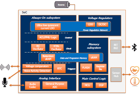
Figure 1-1: Standard SoC architecture in IOT applications
The Always-ON domain in a SoC is the first part of the circuit supplied at power-up, and it remains powered whatever the SoC mode, until the whole system is completely shut down. It manages the boot sequence and the transition between each SoC mode. Depending on the target application, AON power domains will contain the following blocks:
- ACU (Activity Control Unit) or ePMU (embedded Power Management Unit) is the logic control block of the SoC, in charge of the control of the start-up of the SoC as well as the transitions between SoC modes, e.g. turning on/off power domains and their associated clocks and supplies.
- Triggers allow monitoring the events used to wake-up the SoC, along with the elements related to the SoC infrastructure (power supply, clock, I/O...). Such wake up events can be generated in various ways:
- Voltage comparators allow to wake up the SoC with an analog input voltage (RF Analog, RFID event…)
- Real Time Clock (RTC) provides an accurate time counting allowing to wake up the SoC at regular time intervals (each second, minute, day or month depending on the application duty cycle).
- Voice activity Detection (VAD) allows to wake-up a SoC when a voice (surveillance applications) or a key word is detected (“ALEXA”, “Hey SIRI”, “OK GOOGLE…)
- Wake-up pin allows to manage system wake-up from blocks external to the SoC, by the means of a general-purpose I/O (GPIO) powered in sleep mode
- Visual/face detection, fingerprint detection…
- Oscillators provide the clock frequency to the triggers and the ACU/PMU. To reduce current consumption of the AON domain, the frequency provided is slower than the system frequency. The AON domain frequency varies between a few kHz to a few MHz. Two types of oscillators can be used in AON domain:
- Crystal (XTAL) oscillator which gives an accurate frequency based on an external crystal.
- RC oscillator which is less accurate with a fast startup-time, and allows reducing the SoC BoM cost as it does not require an external crystal.
- Retention memory allows storing data such as latest configuration settings, or signal measurement results during sleep/power-down modes. The SRAM is one of the main contributors to leakage in power-down modes, it thus makes sense to not power it in such idle modes.
- Ultra low-quiescent LDO provides the regulated voltage from the battery to the Always- On domain. In some applications where the always-on domain only comprises the ACU/PMU, using specific standard cells directly supporting the battery voltage can bring advantages by removing the need for a voltage regulator.
Each application has its own needs and market requirements for consumption in sleep mode. It is thus necessary to choose the appropriate always-on architecture for each application. The following table aims at helping to select the correct and most competitive architecture for the AON domain depending in the final user application:
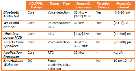
Table 1: Always-On domain blocks and typical current application in various applications
2. Why reduce the current consumption of AON domain?
2.1. Average current consumption and battery autonomy
The following figure represents how to compute the key parameter of the battery autonomy which is the average current consumption:
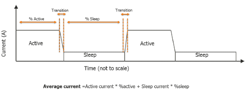
Figure 2-1 : Average current consumption

Note that the equation to compute the average current consumption is given in Figure 2-1.
The equation parameters are defined as:
- Battery Autonomy represents the life duration expressed in hours/days/years
- Battery capacity is expressed in mAh
- Sleep current is the current in sleep mode, essentially represented by the always-on domain current and the leakage of other blocks
- % active and % sleep represent respectively the percentage of time spent in active and sleep mode
Note that to simplify the equation the current wasted during transitions is not considered. However, optimizing the duration of mode transitions is essential to reduce the overall power consumption of a SoC by reducing the power wasted when transitioning from one SoC power mode to another.
2.2. Impact of sleep current consumption on battery autonomy

Table 2: Impact of sleep current consumption in a coin-cell battery powered application in active mode 15 minutes per day (1% active, 99% in sleep mode).

Table 3: Impact of sleep current consumption in a coin-cell battery powered application in active mode 1 minute per day (0.07% active, 99.93% in sleep mode).
The two previous tables show how important it is to improve the current consumption in sleep mode, depending on the application and activity scenario. It can allow increasing battery autonomy from a few days to a few years. Note also that the sleep mode current can also be a marketable performance, so it can be needed to achieve an ultra-low number even if it doesn’t impact battery autonomy. Battery autonomy can be directly computed by identifying the operation modes and their respective current consumptions.
2.3. Decreasing current consumption in sleep mode
In conventional RF communication applications, at battery power level: 50 % is dedicated to active mode (reception/transmission), 20 % to data storage and system maintenance and 30 % for sleep mode. Previous tables show how sensitive the battery autonomy is to active current, sleep current and percentage of time spent in each mode. Taking that into account, SoC architectures are designed so that energy-consuming blocks spend the smallest possible time in active mode. To increase battery autonomy, the 2 following solutions can be combined:
- Minimizing sleep mode power consumption with an improved architecture for alwayson domain and using ultra low-power blocks
- Minimizing current consumption wasted during transitions thanks to faster transitions
The minimization of sleep mode power consumption indeed involves paying attention to the construct of the Power Regulation Network (aka PRNet). The selection of the voltage regulator(s) is critical in itself as they may contribute to more than 50% of the power consumption in sleep mode, when only the blocks in the always-on domain are active. Furthermore, enabling the always-on domain to operate at very low voltage may significantly decrease the power consumption while saving silicon area and BoM costs.
3. Different implementations to meet the SoC challenges
There is not a unique solution to define the architecture corresponding to a given set of needs. As an illustration, we will consider the following example:
- The SoC needs a calendar function to track date and time during the operating lifetime. The AON domain needs a Real-Time Clock (RTC) with calendar feature and its associated low-frequency oscillator (32.768 kHz).
- The SoC can be woken-up either by an interrupt signal or by an analog event (voltage becoming higher than a given threshold). At least one GPIO is required to receive the interrupt signal. An analog comparator is also required.
- The SoC has to memorize some data during the idle mode (data “propagated” from one iteration of the active mode to the following). Part of the embedded memory remains in retention mode to save this data.
- During the idle mode, the SoC has to control the state of a companion chip. At least one GPIO is needed to send a signal out of the SoC.
- The Rest-of-SoC (RoS) is OFF during idle modes, as well as the related regulators.
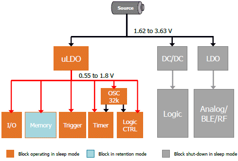
Figure 3-1: Always-On standard architecture at 55 nm
3.1. Description of the architecture of the example
Figure 3-2 illustrates the reference architecture to build the different possible synopses.
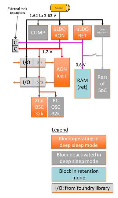
Figure 3-2: Reference figure for the different synopses
Two oscillators are considered to generate a clock signal for the RTC and the AON logic:
- A crystal-based oscillator (Xtal OSC) allows delivering the accurate, low-power and low-drift clock required by the calendar function of the RTC.
- The RC OSC enables to clock the AON logic during the SoC start-up to compensate the long start-up time of the crystal-based oscillator (typically some hundreds of milliseconds). Once the other oscillator is settled, the RC oscillator is disabled.
A 2kx32 (8 kB) retention RAM is considered to retain relevant data during idle modes at a minimum leakage cost. One of the challenges of the architecture is to select the appropriate supply voltage to obtain the overall lower leakage.
While the memory is in retention mode, the uLDO is enough to deliver the appropriate amount of current. In active mode, when the memory is operating at full speed, the uLDO may not be able to deliver the required current. In this case, the memory is supplied in active mode by one of the regulators used to supply the Rest-of-SoC (represented in Figure 3-2 by the “other regulators” box). A switch enables to perform the connection between this regulator and the memory.
In the following synopses representing different implementation possibilities, the following conditions are considered:
- The SoC is mainly operating in deep sleep mode; which is the mode we will optimize. The comparator is OFF, only its area is considered.
- Different figures, such as area and power consumption, are based on Dolphin Integration’s Silicon IPs in 55 nm processes. The list of these Silicon IPs is given at the end of the article.
- The Rest-of-SoC contains one DC/DC (to supply the core logic) and one LDO (to supply analog features such as a PLL or RF transceiver). This implies that one inductor and two capacitors are required on-board. The case where an LDO is used to supply the core logic is discussed later in this article.
- The Rest-of-SoC area is 10 mm2.
- The Rest-of-SoC leakage in deep sleep mode is 500 nA, including leakage of dedicated regulators and I/Os.
We consider 500 nA for the latest figure in each synopsis, mainly to simplify the description.
In some of the following synopses, this leads to neglecting:
- The leakage of blocks composing the logic core which are supplied in some cases and powered-off in others
- The leakage of the regulator supplying the logic that may vary depending on the voltage at its output (case when this regulator is associated with another): the Ioff current of the power stage decreases as the voltage across the power stage (input voltage – output voltage) is reduced.
Depending on the characteristics of the above listed blocks, some variations more or less compensate each other. In the context of a “real SoC”, a more rigorous analysis has to be performed.
3.2. Possible implementations
Different possible implementations of the architecture can be designed.
The first change is to replace the switch connecting the retention RAM by a supply multiplexer (named MUX in Figure 3-3). The aim of this MUX is to provide a secure transition for the supply rail in normal operation to the supply rail in retention mode in order to prevent data corruption due to uncontrolled voltage drops.
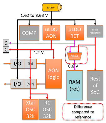
Figure 3-3: Synopsis #1, direct implementation with a supply multiplexer (#1-mux)
A possible gain in terms of area and BoM can be achieved by using a single regulator to supply both the AON logic and the retention RAM (Figure 3-4). The drawback is an increase of the RAM leakage due to the increase of its supply voltage from 0.6 V to 1.2 V. Depending on the saving on the quiescent of the removed regulator, the power consumption increase in deep sleep mode can be more or less significant.
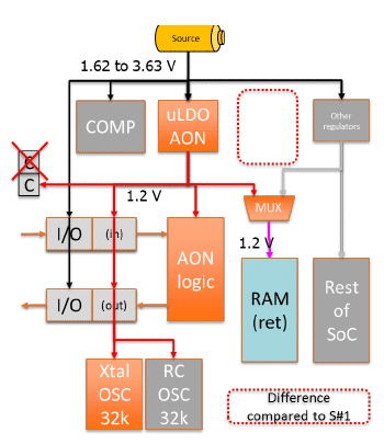
Figure 3-4: Synopsis #2, single regulator to supply the AON logic and the retention RAM (#2-1uLDO)
As a supply multiplexer may not be available, an alternate possibility is to associate in parallel the regulator delivering the current to the RAM in normal mode, with the uLDO supplying the RAM during idle modes. This association is named a Retention Alternating
Regulator (RAR) in Dolphin Integration’s offering. Its output rail is used to supply both the RAM and a part of the Rest-of-SoC (logic core for instance) as illustrated in Figure 3-5. In terms of BoM, it also saves one capacitor as the uLDO shares the capacitor already used by the other regulator. In terms of safety, a dedicated controller is provided in Dolphin Integration’s RAR to automatically sequence the change from one of the associated regulators to the other.
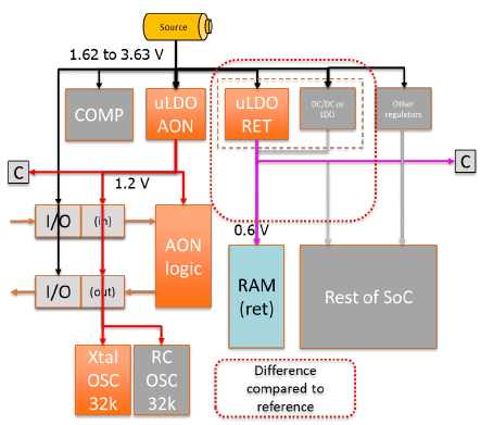
Figure 3-5: Synopsis #3, Retention Alternating Regulator (RAR) supplying retention RAM and a part Rest-of-SoC (#3-RAR)
A possible improvement of the dynamic power consumption in idle mode consists in using a Near-Threshold Voltage (NTV) standard cell library to supply the AON logic together with the retention RAM (Figure 3-6). This allows reducing the dynamic power consumption. A uLDO is still required to supply the core voltage of GPIO when using a regular I/O library.
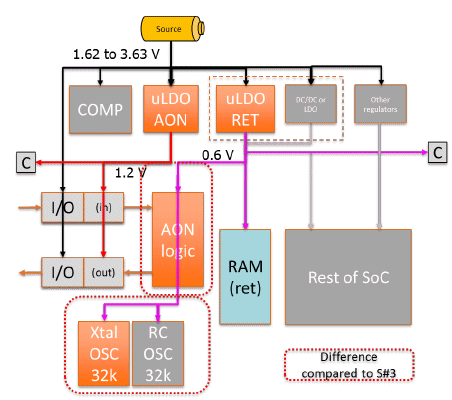
Figure 3-6: Synopsis #4, RAR and NTV library (#4-RAR-NTVlib)
If AON logic leakage is an issue, a standard cell library using I/O MOS devices may be the relevant solution (Figure 3-7). Supplying the AON logic directly on the battery rail has an impact on dynamic power consumption that has to be considered. As in Figure 3-6, a dedicated uLDO is still needed to supply the core voltage of GPIOs. A hidden advantage is that the function inside the AON logic that controls the regulators can directly interface with them without requiring level shifters, leading to a possible simplification of the UPF description.
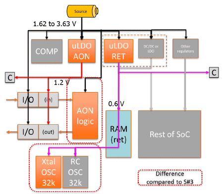
Figure 3-7: Synopsis #5, RAR and I/O MOS library operating at battery voltage (#5-RAR-BATlib)
Some synopses can be improved depending on the availability of dedicated I/O libraries enabling to remove regulators required to supply the GPIO pre-driver rail at core voltage.
This is illustrated in Figure 3-8 if the I/O library is able to operate at the same voltage as the NTV library, and in Figure 3-9 if the I/O library is able to fully operate at the battery voltage.
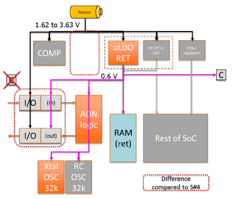
Figure 3-8: Synopsis #6, using NTV library and IO-to-NTV GPIOs (#6-RAR-NTVlib&IO)
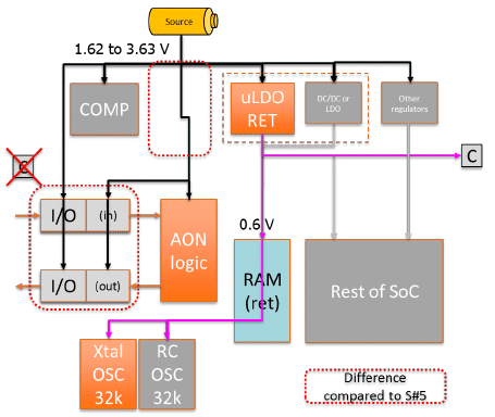
Figure 3-9: Synopsis #7, using I/O MOS library and IO-to-IO GPIOs (#7-RAR-BATib&IO)
3.3. How to select the most appropriate implementation?
As many possible solutions can be imagined, there is a need for a tool enabling to objectively assess and compare them in order to select the one achieving the best performances. A methodology based on a Figure of Merit (FoM) is perfectly suitable in such a case.
3.3.1. Figure of Merit (FoM) definition
The main advantage of a FoM is to be adaptable to each SoC. By defining the performances of interest for a given SoC (among silicon area; power consumption either in a specific mode or over the application lifetime; cost of on-board components…) and by giving a weight to each one, it is then possible to sort them depending on their overall performance. The FoM formula, with the performances listed before, has the following equation:
![]()
Equation 3.1: FoM formula considering area, power and BoM
- The power consumption is considered at the level of the main supply source. Considering the power consumption (in Watts) or the current consumption (in Amps) is equivalent in the FoM perspective, users must just take care not to mix the units.
- Ideally, the area is the one of the entire SoC. In some cases, only a subset of the SoC, like the power management network, can be considered if some data is unknown. But the same scope must be used for each synopsis to be compared.
- The BoM can be used to also consider the on-board area if it is critical for the application (small board requirement, small in-package space...)
- The weights (Wa for area, Wp for power, Wb for BoM) depend on the challenges the SoC has to deal with for the application and the sum of the weights equals 100 %. For instance, if the main challenge is power consumption, Wp will have the highest weight.
To have a faster reading, the different FoM results can be normalized to the lowest computed value. If two results are respectively 1 and 1.25, it is fast to assess that the best synopsis (the one having a FoM equal to 1) is 25 % better than the second synopsis.
Some other performances can be easily added if they are critical for the application, as for example the transition time needed to switch from one mode to another. The FoM from Equation 3.1 can be updated as follows:
![]()
Equation 3.2: FoM formula considering area, power, BoM and transition time
With such equations, the best solution to meet the required performances is the one having the lowest value. We consider Equation 3.1 to illustrate this article.
To obtain relevant results, the typical consumption has to be considered for the FoM computation. Considering that the maximum current is not representative of the average behavior of the SoC over the application lifetime and may mask the contributions of several blocks to the average power consumption. Nevertheless, the maximum current is a critical information to make sure that the regulators are correctly selected.
FoM calculation can be considered as a 2-step process:
- First, compute the power consumption, area and BoM for each synopsis, the most complicated being the power consumption.
- Then, aggregate all these figures to compute the FoM of each synopsis.
The FoM results are computed with the power consumption having a high priority, followed by the area. The BoM has the lowest priority. In terms of weights, this gives:
- Area weight, Wa: 25 %
- Power consumption weight, Wp: 60 %
- BoM weight, Wb: 15 %
3.3.2. Figure of Merit of the 5 first synopses
We can draw a first selection by only considering that regular I/Os are available (the 5 first synopses). Figure 3-10 gives details on the contributions of the different blocks to the current consumption in deep sleep mode. The current consumption is considered at the battery level.
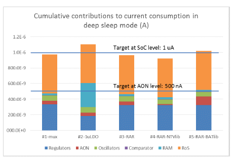
Figure 3-10: Current consumption of synopses using regular I/Os
When considering the 500 nA mentioned in the previous section for the Always-On domain in association with the 500 nA for the RoS (Rest-of-SoC), 3 of the synopses match as the overall SoC current consumption is lower than 1 uA.
Synopsis #2 has the highest current consumption, as the gain on the contribution of regulators (one regulator removed) is not sufficient to compensate the increase of the RAM leakage when increasing its retention voltage. For a smaller RAM size, this synopsis would probably have the best current consumption (i.e. the lowest). For higher RAM sizes, the leakage would become the main contributor, highlighting the interest of using the lowest possible retention voltage.
For synopsis #5, the increase of the current consumption of the AON logic is not compensated by another block. The consumption increase is due to the dynamic consumption as the logic block operates at 3.3 V.
Synopsis #4 has the lowest current consumption due to a reduction of both dynamic consumption and leakage of the AON logic operating at 0.6 V, thanks to the NTV library (Near Threshold Voltage library).
Figure 3-11 gives an overall view of the different FoM results and the relative contributions of area, current consumption and BoM parameters.
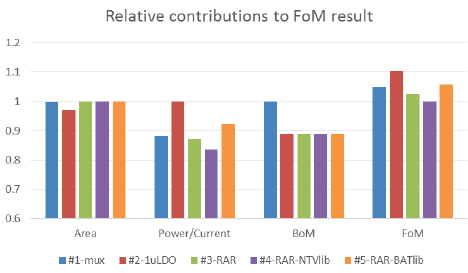
Figure 3-11: FoM details for synopses using regular I/Os
Regarding area, synopsis #2 has the lowest one. But this synopsis also has the highest current consumption as previously described. All other synopses have a similar area. Regarding BoM, synopsis #1 has the highest one. Synopsis #2 enables saving 1 capacitor as one regulator is removed. Other synopses enable saving one capacitor as the two associated regulators share the same capacitor.
Regarding the ranking of the different synopses:
- Synopsis #4, using NTV library, has the best FoM (lowest value). It has the best current consumption and a similar area and BoM as others.
- Synopsis #3 has the second rank for FoM and current consumption.
- Synopsis #1 has the third rank, even if its BoM is the worst and its area and current consumption are average.
- Synopsis #5 has the fourth rank, the same as its current consumption (the second highest).
- Synopsis #2 has the last rank, the gain on area does not compensate its current consumption (the worst).
The definition of the weights is important and must reflect the needs and challenges that must be reached at SoC-level. As an example, if we rearrange differently the weights, the ranking will be different and the distance between the synopses will become more or less significant. In the case illustrated here, the selected weights give the highest distance. Allocating the 60%, 25% and 15% to other terms of the FoM may cause the distance to be reduced by about 3. Here, synopses #4 and #3 will always remain at the top positions, but in other contexts, the ranking can be completely modified. With Wa = 15 %, Wp = 25 %, Wb = 60 %, synopsis #5 has the third rank and the difference between the 3 first synopses is reduced.
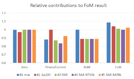
Figure 3-12 : FoM results with different weights
3.3.3. Impact of dedicated I/O libraries on the Figure of Merit results
Now, let us consider at the same time the two synopses involving dedicated I/O libraries. Figure 3-13 includes the current consumption of these two synopses for comparison with the other synopses.
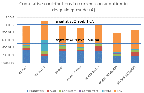
Figure 3-13: Current consumption of synopses using either regular I/Os (#1 to #5) or dedicated I/Os (#6 & #7)
Synopsis #6 has the same benefit as synopsis #4 regarding the current consumption of the AON logic due to operating at the retention voltage, thanks to the use of an NTV library. It also has the lowest overall current consumption due to the removal of the regulator previously dedicated to supplying the core voltage of GPIOs.
Even if using a library operating at battery voltage causes the highest dynamic consumption of the AON logic, the removal of one regulator thanks to the use of dedicated GPIOs enables reaching the second lowest current consumption.
From a FoM perspective, these two synopses enable significant improvement, as illustrated in Figure 3.3-14.
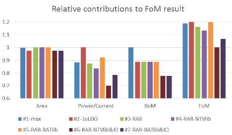
Figure 3.3-14: FoM details for synopses using either regular I/Os or dedicated I/Os
Synopses #6 and #7 have similar area as synopsis #2 due to the removal of one regulator. But as they also embed an association of regulators in parallel, this also enables having the lowest BoM by saving one additional capacitor device.
In terms of FoM:
- Synopsis #6 has the first rank as it has the best figure for each criterion.
- Synopsis #7 has the second rank.
- Other synopses have their previous rank incremented by two.
This shows, in the context of the chosen example, the potential benefit enabled by using dedicated I/O libraries to operate either with an NTV library or with a library operating at the battery voltage.
Just as a comparison, this impact of weights is lower in such a case, as, for each criterion, the two latest synopses have the best performances. With a different weighting, such as Wa = 60 %, Wp = 15 % and Wb = 25 %, the ranking remains unchanged.
3.3.4. How to select the appropriate regulator for active mode?
Until now, we have just considered the deep sleep mode. Let us now also consider the active mode.
Activity duty cycle has an impact on the selection of the regulator supplying the core logic of the Rest-of-SoC, as discussed in section II.
Using the average power consumption in the FoM computation enables checking whether using either a DC/DC or an LDO regulator is the most appropriate to supply the core logic. To illustrate this, let us consider a simplification of synopsis #4 as illustrated in Figure 3-15.
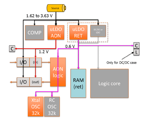
Figure 3-15: Example to illustrate the selection of either DC/DC or LDO, based on FoM
In deep sleep mode, we still consider a 1 uA consumption at battery level. In active mode, the logic core + RAM + AON logic is considered as one single figure, named as core logic power consumption. We consider different cases where this figure varies between 100 uA and 20 mA.
We also consider different activity duty cycles, from 1 second per day of operation in active mode to a few minutes.
For the SoC area, we arbitrarily consider a 10 mm2 SoC total area when a DC/DC is used, and 9.5 mm2 when an LDO is used.
For the BoM, we consider 2 capacitors and 1 inductor when a DC/DC is used, and 2 capacitors when an LDO is used.
For simplicity, we consider that the DC/DC efficiency is 85 % whatever the output current it provides.
Considering 99.99 % of the time in deep sleep mode and 0.01 % in active mode corresponds to about 9 seconds of operation per day. Figure 3-16 illustrates the variation of the FoM as a function of the current consumption of the logic core in active mode.
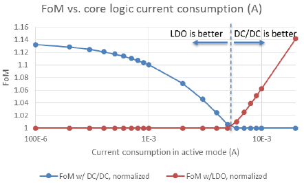
Figure 3-16: DC/DC vs. LDO FoM, 0.01 % ON activity (the lower, the better)
For a current consumption of the logic core up to 4.5 mA, using an LDO gives the best FoM thanks to the lowest area and BoM. For higher current consumption, the improvement achieved on current consumption when using a DC/DC compensates for the area and BoM penalty.
Figure 3-17 illustrates the case for about 1 second of operation per day (99.999% of the time in deep sleep mode, 0.001 % in active mode).
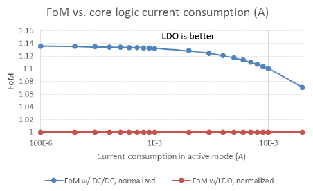
Figure 3-17: DC/DC vs. LDO FoM, 0.001 % ON activity (the lower, the better)
With such an activity duty cycle, using an LDO is always the best choice if the current consumption remains in the considered range. For a 100 mA current consumption, a DC/DC would be the best choice.
Figure 3-18 illustrates the case for about 1 minute and a half of operation per day (99.9% of the time in deep sleep mode, 0.1 % in active mode).
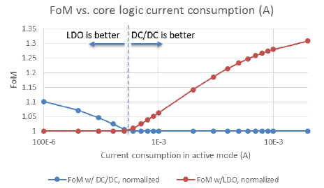
Figure 3-18: DC/DC vs. LDO FoM, 0.1 % ON activity (the lower, the better)
Compared to the case with 0.01 % of the time in active mode, the pivotal value decreases to about 450 uA. The longer the time spent in active mode, the better the choice of using a DC/DC is, as the current consumption in active mode becomes preponderant over the current consumption in deep sleep mode.
4. Using ultra low power components
The FoM results of the different synopses are computed from data based on Dolphin Intgeration’s products in 55 nm processes. They are listed in the following table:
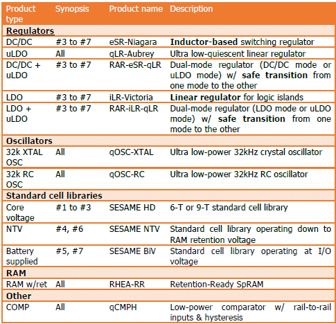
Table 4.1: Products used as input data for FoM computation
Some other products are not represented in the synopses, but are relevant for low-power SoCs.
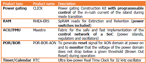
Table 4.2: Other products suitable for low-power SoC
5. Conclusion
This article has described the challenges related to designing an Always-On domain for power efficient sleep mode. It has also presented different possible synopses for a given set of needs. The FoM-based methodology has been illustrated to enable selecting the one fitting the challenges of the SoC in terms of power/current consumption, area and BoM. It has also demonstrated that the FoM approach is generic and can be extended with other parameters to consider other challenges, such as for instance the transition time.
Moreover, this article has highlighted the improvement that standard cell libraries operating either near to threshold voltage (NTV) or at battery voltage can bring for optimizing the Always-On domain of a low-power SoC. It is even better when associated with dedicated I/O libraries.
About the authors
Sebastien Genevey
 Sebastien Genevey received the Master's Degree in Integrated Circuit design from the Polytechnic Institute of Montpellier, France. He enters to Dolphin in 1997 as analog designer for mixed-signal products. He is currently analog architect for the different products lines and supports the sales team as system architectural expert. sge.jazz@dolphin.fr
Christian Dominguez
 Christian Domingues began his semiconductor career at the Techniques of Informatics and Microelectronics for Integrated Systems Architecture (TIMA) laboratory. Since 2006, he has been involved in Dolphin integration respectively as a mixed signal design architect and application engineer manager, working in the field of high-performance measurement ΣΔ ADCs and power management. He received a master’s degree and a PhD from the Polytechnical National Institute of Grenoble (INPG) in France in 2001 and 2005, respectively. christian.domingues@dolphin.fr
Related Semiconductor IP
- UFS 5.0 Host Controller IP
- PDM Receiver/PDM-to-PCM Converter
- Voltage and Temperature Sensor with integrated ADC - GlobalFoundries® 22FDX®
- 8MHz / 40MHz Pierce Oscillator - X-FAB XT018-0.18µm
- UCIe RX Interface
Related Articles
- Improving design turn around time on a complex SoC by leveraging a reusable low power specification
- Novel and efficient power grid design for lesser metal layer process SOC's
- An ESD efficient, Generic Low Power Wake up methodology in an SOC
- Accurate and Efficient Power estimation Flow For Complex SoCs
Latest Articles
- A Scalable Open-Source QEC System with Sub-Microsecond Decoding-Feedback Latency
- SNAP-V: A RISC-V SoC with Configurable Neuromorphic Acceleration for Small-Scale Spiking Neural Networks
- An FPGA Implementation of Displacement Vector Search for Intra Pattern Copy in JPEG XS
- A Persistent-State Dataflow Accelerator for Memory-Bound Linear Attention Decode on FPGA
- VMXDOTP: A RISC-V Vector ISA Extension for Efficient Microscaling (MX) Format Acceleration