Hardware/Software Partitioning and Interface Synthesis in Networks On Chip
Francesco Regazzoni,ALaRI - USI, Lugano, Switzerland
Marcello Lajolo, NEC Laboratories America, Princeton, NJ
Abstract
With deep sub-micron technology, chip designers are expected to create System-On-Chip (SOC) solutions by connecting different Intellectual Property (IP) blocks using efficient and reliable interconnection schemes. On chip networks are quite compelling because, by applying networking techniques to on-chip communication, they allow to implement a fully distributed communication pattern with little or no global coordination. This avoids the problems due to the difficulty of implementing future chips with one single clock source and negligible skew. On the other hand, in order to benefit from the NOC communication paradigm, designers should perform a careful functional mapping for taking advantage of spatial locality, by placing the blocks that communicate more frequently closer together. This reduces the use of long global paths and the corresponding energy dissipation. In this work we show how a tile based NOC architecture can be exploited in order to support a flexible hardware/software partitioning of a system-level specification and we present a methodology for the automatic synthesis of the hardware/software interfaces.
1 Introduction
With billions of transistors switching at GHz frequencies, the problem of getting signals across a large die is becoming very complex. Timing, signal integrity and power issues are all escalated to a new level. The major challenge that silicon technologies are facing is that on-chip synchronization with a single clock source and negligible skew is no longer possible. The problem is exacerbated by the fact that the design of System- On-Chips (SoCs) is more and more based upon reusable IP cores in order to meet stringent time-to-market requirements. In this context, after the IP cores are identified, the focus shifts on the integration challenge that involves the need to build a working system from a collection of cores that were not designed to work together. The amount of logic required in order to adapt incompatible protocols make global on-chip communication even more complicated.
Hierarchical communication-centric system architectures based on the GALS (Globally Asynchronous Locally Synchronous) paradigm target the aforementioned design challenges and communication bottlenecks [1] and Networks On Chip (NOCs) offer an ideal application scenarios for GALS concepts [2]. NOCs propose to localize functions in small computing platforms tuned to specific classes of tasks. Those computing islands are then bridged with an efficient data communication structure to be able to work in parallel on a common application. Several proposals for NOC architectures have been presented: MANGO [3], SOCBUS [4], RAW [5], HiNoC [6] and NTNU [7] (among others). In this work we propose a wrapper organization for tile based NOC architectures and we show, by means of an example, how to approach the hardware/software partitioning and interface synthesis phases in order to take advantage of the new NOC paradigm. We also discuss suitable routing algorithms and flow control techniques necessary to provide predictable latency to on-chip communications and we propose a programming model for NOCs.
The content of this paper is structured as follows. Section 2 presents our tile wrapper architecture and discusses its features and properties. Section 3 presents our hardware/software partitioning strategy for tile based NOCs. Section 4 introduces some interface synthesis related aspects. Section 5 presents an example of application. Section 6 concludes the paper.
2 Tile based NOC architecture
Figure 1 shows on the left side a typical 2-D mesh interconnection topology. The architecture consists of multiple tiles organized in a Manhattan-like structure. Tiles are wrapped with a tile wrapper that provides access and isolation to each tile. The NOC is homogeneous when all tiles are identical, and heterogeneous when each tile can contain a different set of architectural elements like processors, buses and hardware peripherals.
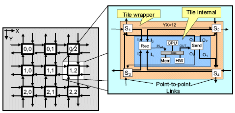
Figure 1: 2D mesh NoC architecture.
A tile is a computation or storage unit or their combination. Typical examples would be embedded processors and DSP cores provided with caches as well as local memories, and both dedicated and configurable hardware resources. A tile wrapper routes and buffers messages between tiles. Each tile wrapper is connected to four other neighboring tiles through input and output channels. A channel consists of two one-directional point-to-point links between two tile wrappers. A tile wrapper might have internal queues to handle congestion.
On the right side of Figure 1, the internal organization of our tile is shown. We have four switches (S1 to S4), one at every corner of the tile and dedicated receiver (Rec) and sender (Send) units that act as adaptation layers between the wrapper, that is the same in every tile, and the internal tile, that instead can be different in every tile. The internal tile might contain multiple buses and processors and the only assumption is that one single bus will be allowed to be connected to the tile wrapper.
The NOC architecture provides the communication infrastructure for the tiles. The two main objectives behind the NOC architecture are:
- It is possible to develop each tile as a stand-alone block and create the NOC by connecting the blocks as elements in the network.
- The network is highly scalable and configurable so that it can be adapted to the needs of different workloads, while maintaining the generality of application development methods and practices.
It is realistic to expect that the area of a tile is the maximal synchronous region in a given technology. It is expected to shrink with every new technology generation. Consequently, the number of resources will grow, the tile-to-tile bandwidth will grow, but the network wide communication protocols will not be affected. The most suitable model of computation for this system is a heterogeneous network of resources executing local computation. Tiles operate asynchronously with respect to each other. Synchronization is provided by synchronization primitives which are implemented by passing messages over the network. Even a non-local memory is accessed through message passing.
2.1 Routing constraints
In our tile wrapper, each switch has three incoming links, as shown in Figure 1. The incoming connections are the following:
1. Outside: packets coming from an adjacent tile.
2. Straight: packets coming from an adjacent switch inside the same tile.
3. Internal: packets generated in the same tile.
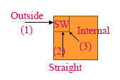
Figure 2: Incoming links.
Similarly, each switch has three outgoing links, as it is shown in Figure 3. The outgoing connections are the following:
1. A packet coming from the Outside input can go in any of the three possible directions:
- it can turn left;
- it can go straight to the adjacent switch in order then to exit in that direction;
- it is sent internally when it has reached its final destination.
2. A packet coming from the Straight input can only go outside:
- it comes from an adjacent tile.
3. A packet coming from the Internal link can only go outside:
- the sender unit has selected the tile based on the direction in which it wanted to send the packet out.

Figure 3: Outgoing links.
2.2 Routing algorithm and flow control
Due to the limited amount of buffering and data acceptance between routers in a NOC, flow control needs to be added to the routing algorithm. We use wormhole routing, a technique where packets are split into flits (flow control digits) that are forwarded indipendently to the next router as soon as it is ready to accept them.
We use a source-based dimension order routing where each flit follows the same routing path in order to avoid the need to reorder flits at the destination. The routing decision is made in the source node and after that the routing path to the destination is completely deterministic. Dimension-order routing is very simple to implement, but it suffers from the fact that it provides zero adaptiveness that is instead of key importance in NOCs in order to minimize congestion. We add some adaptiveness to the routing algorithm at the source node, where, based on congestion information provided by a backpressure scheme implemented in the tile wrappers, we can choose between minimizing first either the X or the Y distance between source and destination and, in alternative, it is also possible to route packets in one of the two remaining directions. The number of tiles traversed by a packet in order to reach its destination can hence be chosen (traded-off) by taking into account the dynamic congestion on the chip.
3 Hardware/software partitioning in NOCs
We consider a tile based NOC like the one shown in Fig. 1. The NOC is homogeneous and in each tile there is one single processor architecture with processor, local memory and custom hardware, all connected to the same bus. The target system that we want to map onto a tile based NOC can be described at the conceptual level as a constellation of concurrent, interacting subsystems or tasks. Each task communicates with other subsystems and shares the entire memory addressable space that is partitioned among the various tiles. Basic questions that we want to answer for this type of architecture are the followings. How to partition the design to take maximum advantage of multiple processors? How to manage the software among all the processors? How to take advantage of custom hardware?
3.1 Memory abstraction
At the application level the NOC organization is completely abstracted out. Our methodology allows to partition a given application by distributing different sets of tasks onto different tiles. When a task inside one tile generates addresses belonging to the address space of that tile, the communication remains local to that tile and it is handled internally without involving any operation in the tile wrapper. When instead a task inside one tile generates an address destined to a task that is mapped onto another tile, the sender unit will send a word of data to one of the four adjacent tiles based on the routing algorithm, in order to reach the destination tile. At the destination, the receiver unit will receive the packet and send it to the internal bus. A packet coming from one tile and going to another tile might traverse different tiles based on the the routing path chosen. In all the intermediate tiles, the packet will only be handled in the wrapper, that will simply route it left or straight, without involving any internal operation.
4 Interface synthesis in NOCs
Intertask communications are built on two foundations: the software communication mode and the corresponding hardware mechanism. The are two basic communication styles: message passing (point-to-point connection in hardware) and shared memory.
In a NOC, the global communication on the chip is provided by the on-chip network once packets are generated, but interface synthesis is still needed in order to provide intra-tile communication for tasks mapped onto the same tile. Moreover, for inter-tile communications, it is necessary to configure the sender units in order to route the communication. Based on the addresses of messages and shared memory accesses, a sender module needs to figure out the destination tile of the communication and select the appropriate direction in which to send the packet. The sender module needs also to packetize the information to be sent based on the transaction generated on the internal bus. We configure each sender unit by means of a lookup table that is stored in a memory tightly coupled with the sender. This memory is loaded at system initialization based on the output of the interface synthesis tool and acts as a set associative memory of addresses that the sender has to lookup on the internal bus and route externally to the tile.
5 Case study
In this section we present an example of mapping of a H.263 video encoder [8]. It is important to underline that the size and the overall complexity of this system does not justify the need for a NOC instead of a traditional bus-based architecture. However, we have chosen this system since it has some characteristics that make it interesting when a NOC implementation is considered.
The encoder was partitioned into four processes and it uses six memory blocks. The processes are: DCT which performs the zig zag scan and the Discrete Cosine Transform; IDCT which reverses the zig zag scan and calculates the Inverse Discrete Cosine Transform; APP which computes the remaining parts of the algorithm and performs the global coordination, by reading input frames from the memory Input Buffer and storing the output frames at the end of the compression in the memory Output Buffer; START which gives the signal to start the compression.
The memories are: Input Buffer which stores the input frames to be compressed; Output Buffer, where the output frames are stored at the end of the compression; and memories from M1 to M4 that are used to pass intermediate results between the tasks while performing the compression. Communications among tasks represented with an explicit pointto- point connection are implemented using message passing, while memory blocks are used for shared memory communication.
Figure 5 shows a possible mapping of this video encoder on a tile based NOC. START is implemented as software on Tile (1,0); APP is implemented as software on Tile (1,1); DCT is implemented as hardware on Tile (0,1); IDCT is implemented as hardware on Tile (2,1). The idea behind this partitioning choice is first of all to implement the APP block in software and only offload into hardware the DCT and IDCT blocks, since they are the most time consuming. The fact instead that DCT and IDCT are not placed in the same tile where APP is located is purely intentional in order to describe different aspects of the NOC organization, but there is no specific architectural motivation behind this choice.
The memories are placed with the basic intention to put the data to be processed by one module close to it in order to avoid the need to retrieve them from a different tile. Read operations across different tiles are in fact quite time consuming because
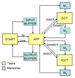
Figure 4: H.263 video encoder architecture.
a read request needs to be sent first from one tile to another and then the retrieved data needs to travel back to the module which requested it. An inter-tile write operation is instead more efficient because it involves only one transfer from the source to the destination tile. This is the main reason why a NOC organization tends to perform well with applications that involve streaming, but it suffers with other kinds of applications that require many modules to access the same piece of data in a temporal order that cannot be statically predicted. In this example, Input Buffer is input to the APP block, so that it is placed on the same Tile (1,1). M1 is input to the DCT block, so that it is placed on the same Tile (0,1), etc.
After the mapping is done, interface synthesis can start. Our interface synthesis tool allows to configure the address space associated to every tile. In this case we have used a convention in which the MSB of the addresses corresponds to the tile’s index: addresses in Tile 1 starts with 0x1, those on Tile 2 will start with 0x2, etc. This convention allows an easier debugging of both interface generation and run time behavior of the system, but it is not a strict requirement of our methodology. The only constraint is that address ranges of different tiles do not overlap. A summary of the output of our interface synthesis tool is shown in Figure 6. The algorithm scans all point-topoint connections in the system and, based on source and destination tiles, generates source and destination addresses for each connection and configures the sender units in all tiles in order to allow them to send out the communication when it is destined to a different tile. For communications through shared memories, instead, the sender receives already the destination address and no conversion is involved.
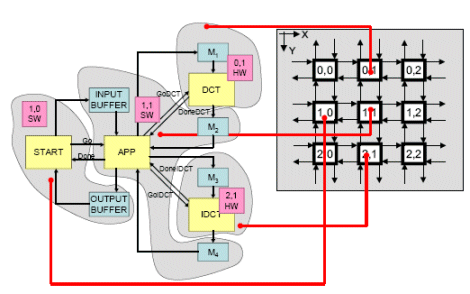
Figure 5: Mapping of the H.263 video encoder on a tile based NOC.
The sender performs the packet creation, by putting the data to be sent into the payload and the destination address into the header with also additional bits involved with routing and flow control information. The sender takes also care of the conversion of the source address into its corresponding destination address for point-to-point links and it selects the direction in which to send the data based on the routing algorithm. In all subsequent tiles the packet will be routed deterministically without any further address translation. The receiver in the destination tile will then be able to determine that the packet has reached its final destination and it will generate a transaction on the internal bus using the specific destination address extracted from the packet header and the data extracted from the payload.
In the list of connections in Figure 6 all communications are inter-tile, because they involve different source and destination tiles, and they have a memory-mapped kind of implementation. In alternative, it is also possible to specify a point-to-point implementation which results in a long-range link insertion that provides a high degree of customization of a NOC [9]. Additional details about our interface synthesis tool can be found in [10].
6 Conclusions
NOCs are chips that apply networking techniques to on-chip communication. NOCs are a step in the right direction as a solution to on-chip interconnects, but a lot of design decisions still need to be made. It is still necessary to select the granularity of cores, the bus width, the network topology, the storage space organization and what should be synchronous or asynchronous. In this paper we have presented a methodology for supporting hardware/software partitioning and interface synthesis in tile based NOCs. We have provided in-depth details about all the different steps of the design flow and we have shown an example of application.
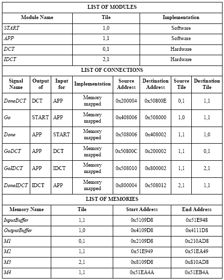
Figure 6: Summary from the interface synthesis tool.
References
[1] S. Moore and G. Taylor and R. Mullins and P. Robinson, “Point to Point GALS Interconnect,” in Proc. IEEE Int. Symposium on Asynchronous Circuits and Systems.
[2] L. Benini and G. De Micheli, “Networks on Chips: A New SoC Paradigm,” in IEEE Computer, pp. 70–78, Jan. 2002.
[3] T. Bjerregaard and J. Sparso, “A router architecture for connection-oriented service guarantees in the MANGO IP Based SoC Design 2005 - December, 7-8 2005 clockless network-on-chip,” in Proc. Design Automation and Test in Europe, pp. 1226–1231, 2005.
[4] D. Wiklung and D. Liu, “SOCBUS: Switched Network on Chip for Hard Real Time Embedded Systems,” in Proc. Int. Parallel and Distributed Processing Symposium.
[5] M. B. Taylor et al., “A Computational Fabric for Software Circuits and General Purpose Programs,” in IEEE Micro, Apr. 2002.
[6] T. Hollstein et al., “A hierarchical generic approach for on-chip communication testing and debugging of SoCs,” in Proc. of the VLSI-SoC.
[7] L. Natvig, “High Level Architectural Simulation of the Torus Routing Chip,” in Proc. Int. Verilog HDL Conference.
[8] “ITU-Telecommunication Standardization Sector. H263 Version 2 (H.263+). Video Coding for Low Bit-Rate Communication,” 1998.
[9] U. Y. Ogras and R. Marculescu, “Application Specific Network-on-Chip Architecture Customization Via Long Range Link Insertion,” in Proc.Int.Conf.Computer-Aided Design, Nov. 2005.
[10] F. Regazzoni and M. Lajolo, “Interface Synthesis in Multiprocessing Systems-On-Chip,” in Proceedings of IP Based SoC Design 2004, 2004.
Related Semiconductor IP
- Bluetooth Low Energy 6.0 Digital IP
- Ultra-low power high dynamic range image sensor
- Flash Memory LDPC Decoder IP Core
- SLM Signal Integrity Monitor
- Digital PUF IP
Related White Papers
- Interstellar: Fully Partitioned and Efficient Security Monitoring Hardware Near a Processor Core for Protecting Systems against Attacks on Privileged Software
- QiMeng: Fully Automated Hardware and Software Design for Processor Chip
- HW/SW Interface Generation Flow Based on Abstract Models of System Applications and Hardware Architectures
- AI, and the Real Capacity Crisis in Chip Design
Latest White Papers
- How Next-Gen Chips Are Unlocking RISC-V’s Customization Advantage
- Efficient Hardware-Assisted Heap Memory Safety for Embedded RISC-V Systems
- Automatically Retargeting Hardware and Code Generation for RISC-V Custom Instructions
- How Mature-Technology ASICs Can Give You the Edge
- Exploring the Latest Innovations in MIPI D-PHY and MIPI C-PHY