Experiences in Formal Checking of a DSP IP Core
by NGUYEN H.N., KOUMOU P. - Bull S.A., METASymbiose S.A.
CANDAELE B., SARLOTTE M., ANTOINE C., EMERIAU S. - THALES Communications
Abstract
This paper describes an experience in applying formal techniques to the verification of system IP cores for a Telecom System on Chip. We discuss the application methods and highlight the complementary aspect with traditional simulation. The paper concludes with comments on the results and a discussion on further improvements of the methods elaborated in this experience.
1. Introduction
Increased use of system IP, such as cores, in the design of SoCs poses new challenges in the verification of IPs to ease the integration effort. However, simulations are extremely time consuming and, as corner cases are becoming increasingly elusive in designs verification tests only cover a small subset of the state space. Recent experiences show that, although strong validation plan on SoC development is performed, buggs/limitations are still discovered later in the product deployment, ex real-time event in network processor [1].
Every design has fundamental characteristics that must hold true during operation. Those characteristics can be defined as properties and checked either statically by means of formal techniques or dynamically during simulation.
This paper describes our experience in applying Model Checking to the verification of DSP IP cores in complement to traditional simulation methods and prototyping methods. The purpose of this experience is to investigate the introduction of a new verification component within the mainstream flow. This will be done by the definition of a methodology and the analysis of potential benefits over traditional methods such as simulation.
In the next paragraph we will describe briefly the architecture of the MEFISTO SoC and then we will relate our experience in applying Model Checking to the verification of the IPs composing this design. Finally we will present some results and conclude with a discussion on further improvements of the method.
The verification work presented has been achieved by a cooperation between Bull, METASymbiose and Thalès within the frame of the Medea+ ToolIP project.
2. The SoC MEFISTO
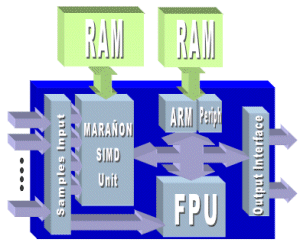
The MEFISTO design targets multiple applications such as smart antenna processing (adaptive beam forming ) and more generally all the application which requires systematic signal processing. The architecture of MEFISTO (Cf. Figure 1) is composed of three main components : A system DSP IP to process fixed point data (Marañon, 1200kgates), a floating point unit (FPU, 400kgates) and an ARM processor to manage the whole system (ARM7™ 100k gates). The FPU has been developed within the Esprit EP27000 OMI Project and has been integrated in the MEFISTO SoC. The design also integrates 1,2Mbits of memory for the 3 cores and achieve 5Gops and 1Gflops.

Figure 1. Architecture of MEFISTO
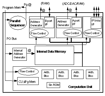
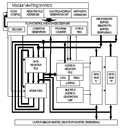
Figures 2 and 3 illustrate hereafter respectively the micro-architecture of the Marañon and the FPU IPs. The design has been targeted in 0.25ì CMOS technology.
3. Formal Verification of MEFISTO
The functional validation of MEFISTO adopts complementary approaches using traditional simulation and formal verification techniques. Simulations are used mostly at circuit levels to check for the correctness of the execution of instructions and to support the overall validation by means of executing pieces of software. In a second phase of the verification, Model Checking[2][3] is used to provide more exhaustive checking and hence to increase confidence in the design. As the purpose of the work is to demonstrate the feasibility and the benefits of Formal Verification, the application of such technique is focused only on some specific features of the design.
- Integer operations including ALU, adder and multiplier of the Marañon core (Cf. Figure 2),
- Family of instructions IADD of the FPU core (Figure 3)
In addition to the application of Model Checking, Equivalence Checking has been also used for the validation of the synthesized net-list (Marañon+FPU) against the golden RTL model.

Figure 2. Architecture of Marañon
It is worth to note that the Formal Verification task has been performed by a team who is not involved in the design task and for whom the specification document represents the unique reference for the design.
These tasks have been achieved with the use of the Model Checker Logan and the Equivalence Checker LEQ developed by METASymbiose.
We detail hereafter the methods used to carried out those verification tasks.

Figure 3. Architecture of FPU
3.1 Verification of the Integer Operations
The verification of the basic arithmetic operations of Marañon are focused on integer operations for which the Model Checker have standard reference models.
3.1.1 Verification of the Adder
As the integer Addition/Minus is performed within one cycle, its verification has been done by means of 7 properties expressed as invariant : The results of the operations together with the expected carry and overflow are formally compared against standard operations.
3.1.2 Verification of the ALU
The ALU has a one cycle depth pipeline, hence its verification has been achieved by means of SCF properties. SCF[3][5] is an outgrowth of STE, hence is suitable to express such a property. The following table described the properties developed for this purpose.
| Op Code | Properties |
| 1111xxxx | Salup=A+B |
| 1010xxxx | Salup=A-B+Cin |
| 01010000 | Salup=B-A with A=X et B=Y |
| 00111100 | cond= (A<=B) with A=X et B=Y |
| 00111000 | cond= (A<B) with A=X et B=Y |
| 001101xx | cond= (A=B) |
| 001100xx | Salup=A+B Salum=A-B |
| 001000xx | Salup=A+B Salum=B-A |
| 00101010 | Salup=ABS(B) |
| 00101011 | Salup=ABS(A) |
| 00011111 | Salup=A if cond=1 else B |
| 00011110 | Salup=B if cond=1 else A |
| 00011011 | Salup=’0..0’ if cond=1 else ‘0..01’ |
| 00011010 | Salup=’0..01’ if cond=1 else ‘0..0’ |
| 0001110x | Salup=’11…11’ |
| 0001100x | Salup=’00…00’ |
| 000101xx | Salup=A |
| 000100xx | Salup=B |
| 000011xx | Salup=A OR B |
| 000010xx | Salup=A AND B |
| 000001xx | Salup=A XOR B |
| 00000000 | Salup=’0..0’ |
Table 1. Properties of the ALU
3.1.3 Verification of the multiplier
A set of 16 properties expressing the different multiplying modes have been developed to check for the correctness of the product operation. The following table describes those properties :
| Op Code | Properties |
| 0 | ACCR = ACCI=0 |
| 1 | ACCR = 2X*Y |
| 2 | ACCI = 2X*Y |
| 3 | ACCR = -2X*Y |
| 4 | ACCI = -2X*Y |
| 5 | ACCR = ACCR + 2X*Y |
| 6 | ACCI = ACCI + 2X*Y |
| 7 | ACCR = ACCR - 2X*Y |
| 8 | ACCI = ACCI – 2X*Y |
| 9 | ACCR = ACCI =2X*Y |
| 10 | ACCR = ACCI = -2X*Y |
| 11 | ACCR = Y |
| 12 | ACCI = Y |
| 13 | ACCR = -Y |
| 14 | ACCI = -Y |
| 15 | ACCR = ACCR + 2X*Y ACCI = ACCI + 2X*Y |
Table 2. Properties of the multiplier
3.2 Verification of a family of instructions of FPU
As mentioned in Section 2, the Formal Verification is not aware of the design details, hence the first step in verification of the instructions was dedicated to determine the starting state of an instruction, i.e. the conditions in which an instruction can be checked statically.
The instruction is then decomposed into a sequence of micro-instructions and the final results in terms of symbolic values of registers and address outputs to memories are checked against expected values. The following sequence illustrated the decomposition of the IADD (Integer Add/Minus) family of instructions :. Cycle 0 : State reset conditions and NOP
. Cycle 1 : Operands coding
. Cycle 2 : Operation and "Parity" coding
. Cycle 4 : Destination coding
. Cycle 5 : NOP
. Cycle 7 : Results Checking
Hence the verification of an instruction is carried out on an interval of 8 cycles. Such a checking is thus suitable to the SCF (STE) concept. All the variables used in the SCF properties are related to observable objects (registers/primary inputs or outputs) of the design.
As FPU is a VLIW processor, the validation of an instruction is accomplished by many properties corresponding to different modes of that instruction. The following example gives the flavor of an SCF property expressing the addition mode on registers of the IADD instruction. The property is expressed in TPL[5] which is a proprietary FPL format of the Model Checker Logan.
Example of a SCF property :
scf opA+B =
(core_flower_inst_flwelr_u1_u7_reg_floc_fsm_1_.0 &
Eq(flwelr_dmo[13:7].0,7'b0000000) &
Eq(mul_pip1[6:0].0,7'b0000000) &
Eq(vliw[119:0].0,
120'h01e0000000000000000000001fff80) &
Eq(vliw[119:69].1,{48'h01e000000000,3'b000}) &
Eq(vliw[66:61].1,6'b000000) &
Eq(vliw[58:0].1,{3'b000,56'h000000001fff80}) &
Eq(vliw[119:4].2,
116'h01e0000000000000000000000bbf8) &
~vliw[1].2 &
Eq(vliw[119:0].3,
120'h01e0000000000000000000001fff80) &
Eq(vliw[119:93].4,{24'h01e000,3'b000}) &
Eq(vliw[90:0].4,
{3'b000,88'h00000000000000001fff80}) &
Eq(vliw[119:0].5,
120'h01e0000000000000000000001fff80) )
=> Eq(Dest[31:0],op1[31:0]) ;
3.3 Equivalence Checking
Finally, in order to provide full confidence on the design process, Equivalence Checking has been applied to the verification of the synthesized net-list (ARM7™ black-boxed) vs. the RTL golden models. This task has been done hierarchically with local flattening when the two hierarchical models present some discrepencies. Some of those discrepencies, mainly due to the optimization of the synthesis tool across the boundaries of the hierarchy, happens to point out unsuspected bugs in the design.
4. Results
The validation of the integer operations requires the development of 25 properties of invariant and SCF types. The computing times take a few seconds to check the properties related to the adder and the ALU and few minutes for the properties related to the multiplier. This validation helps to detect 3 design bugs related to the comparison operations.
The validation of the IADD family of instructions has been done by 15 SCF properties representing different modes. This verification points out some discrepencies between the specification documentation and the realization.
It is worth to recall here that Formal Verification has been applied after the design has been validated by intense simulation and the model used to execute pieces of software. This fact illustrates the advantages of Formal Verification vs. Simulation and particularly highlights their complementary aspect.
5. Conclusions
This paper relates an industrial experience of using Model Checking to validate the system IPs composing a large SoC design. The results tend to illustrate the benefits from this method over traditional simulation and prototyping in detecting corner cases bugs. However, to achieve verification exhaustiveness, the main drawback of Formal Verification is still to face combinatorial explosion. Hence we still consider it as a powerful complementary approach to simulation.
In the design of IPs, and especially for parameterized IPs, such a method provides a powerful validation vector to be transmitted from the providers to the end-users. Its advantage does not focus only on the validation of the IP in stand alone mode but also during its integration in a design.
Equivalence Checking can also contribute to the verification of hard IPs. For this purpose and in order to favor an efficient hierarchical application of Equivalence Checking, clear rules related to naming conventions, FSM coding, ... etc. must be established prior to the application of synthesis.
References
[1] “The barriers between system and SOC”, Candaele B., Sarlotte M., SoC day, Grenoble, May 2002[2] "An Application of Model Checking", Nguyen H.N., Koumou P., DATE'2000.
[3] "Application of Formal Techniques to Hardware and Protocol Verification", Nguyen H.N., Medea Conference, 2000
[4] "Verification of IPs Interconnection" , Nguyen H.N. in SoC Design and Verification Training Course organized by D&R, Grenoble, October 2000
[5] "The Model Checker Logan" Reference Manual. METASymbiose, 2001
Related Semiconductor IP
- ReRAM NVM in DB HiTek 130nm BCD
- UFS 5.0 Host Controller IP
- PDM Receiver/PDM-to-PCM Converter
- Voltage and Temperature Sensor with integrated ADC - GlobalFoundries® 22FDX®
- 8MHz / 40MHz Pierce Oscillator - X-FAB XT018-0.18µm
Related Articles
- Formal Property Checking for IP - A Case Study
- Paving the way for the next generation of audio codec for True Wireless Stereo (TWS) applications - PART 5 : Cutting time to market in a safe and timely manner
- Time Interleaving of Analog to Digital Converters: Calibration Techniques, Limitations & what to look in Time Interleaved ADC IP prior to licensing
- Integrating VESA DSC and MIPI DSI in a System-on-Chip (SoC): Addressing Design Challenges and Leveraging Arasan IP Portfolio
Latest Articles
- An FPGA-Based SoC Architecture with a RISC-V Controller for Energy-Efficient Temporal-Coding Spiking Neural Networks
- Enabling RISC-V Vector Code Generation in MLIR through Custom xDSL Lowerings
- A Scalable Open-Source QEC System with Sub-Microsecond Decoding-Feedback Latency
- SNAP-V: A RISC-V SoC with Configurable Neuromorphic Acceleration for Small-Scale Spiking Neural Networks
- An FPGA Implementation of Displacement Vector Search for Intra Pattern Copy in JPEG XS