eNVM towards 40nm and beyond
eMemory introduces ReRAM IP, qualified at 40nm and extended to 22nm
by eMemory
Introduction
As the semiconductor industry is prominently marching into the nanometer era, fundamental elements face their physical limits significantly, such as electric field across gate dielectric layers, leakage from an ultra-short channel or steep doping profile, newly incorporated leakage/current models, etc. Therefore, numerous techniques have been adopted and applied to transistors, contacts, backend metal routings, or package techniques. Just looking at the transformation of transistors, it abundant new material, process flows, and techniques are incorporated to meet stringent roadmap requirements, like the gate dielectric layer material and effective thickness, the trench isolation stress, ILD strains, the doping techniques of source/drain extensions, or the porous isolation films on top of them. These changes help the transistors meet target specifications with less variation. However, floating-gate Non-volatile memories (NVM’s), the major category of transistor-based elements, have been affected in many ways. For example, charge retention is no longer favorable with gate dielectric thickness or materials; the thermal budget from complex process flow becomes so tight as not to allow changes, not to mention the reliability models of existing devices leave mere a margin for device operations. These factors make the floating gate NVMs more difficult to incorporate into one existing process and may require more unique process modules and flows to gain acceptable electrical characteristics. As a crucial result, the development of embedded floating-gate NVM technology has been hindered at the 40nm platform and beyond for years.
In the meantime, thanks to thousands of materials, processes, devices, and circuit research and studies over the decades, several alternative categories of memories are surfacing [ref. 1], two of which are even becoming possible for commercial production [ref. 2]. These new categories of memories are resistive RAM (ReRAM or RRAM) and magnetic RAM (MRAM). As few suppliers ship standalone ReRAM products, eMemory, as one of the major NVM IP vendors, has been joining the ReRAM IP development with our design and foundry partners, PSCS (Panasonic Semiconductor Solutions) and UMC for years, and is now releasing its first IP this quarter, Q3 of 2021.
Structure & Process module
A typical ReRAM memory cell has a resistive switching element (RSE) electrically connected to the drain of a transistor. Such RSE, arranged as a backend process module, is composed of transition-metal oxide layers stacked between the top and bottom electrodes and encapsulated by isolation material as a tiny cylinder with just a few nanometers’ diameters. Meanwhile, the top and bottom electrodes further connect upwards and downwards to interconnecting metal layers through short via and buffer layers, respectively, Fig. 1. Such transition-metal oxide stack may contain parts of stoichiometric oxide and non-stoichiometric oxide, which provide RSE with a switching characteristic and will be explained with cell operations later. As the top electrode reaches out to a metal line, the bottom electrode electrically connects downwards to a transistor, creating a 1-transistor 1-ReRAM (1T1R).
Furthermore, the Atomic Layer Deposition (ALD) typically forms the RSE stack. With the virtue of such a relatively low-temperature deposition method, ReRAM rarely requires a built-in thermal budget from its process; and easily becomes embedded into various processes compared to others, especially conventional floating gate devices.
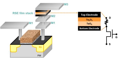
Fig. 1: A typical structure of ReRAM cell
Operation & Mechanism
A ReRAM memory block could store either two states as a typical data storage or multi-level states as a major part of computation in memory (CIM) schemes based on its structural or operational designs. For the bi-state operation, data 0 and data 1 are defined by the resistance of RSE, for example, high resistance state (HRS) for data 0 and low resistance state (LRS) for data 1. There are two major categories of ReRAM, Conductive Bridge RAM (CB-RAM) and Metal-oxide based RAM (OX-RAM). In the CB-RAM category, memory forms as a metal (anode)-oxide-metal (cathode) stack, where the anode metal is prone to be ionized, like silver or copper, and the cathode metal is relatively inert, such as platinum. The CB-RAM gains conductivity from ionized metal ionized from the anode and redistributed/oxidized into the oxide isolation regions. Therefore, CB-RAM is also known as an electrochemical-metallization memory (ECM). On the other hand, OX-RAM applies electrical methodologies to generate oxygen-ion/vacancy from stoichiometric transition metal oxide and redistributes those ion/vacancy into the oxide stack. In this article, we are going to elaborate more on the OX-RAM type.
Moreover, we will combine the conduction mechanism and corresponding operations in this session for an intuitive understanding. To enable the switching characteristics, stabilize it, and re-use it, there are a few steps and flows to be briefed: FORM (forming), PRECYCLE, SET, and RESET.
- FORM (forming): As explained prior, RSE is mainly a stack of stoichiometric and non-stoichiometric transition-metal oxide layers. The stoichiometric oxide is at a very high resistance over mega-Ohms at the fab-out stage. The RSE conducts a relatively low current in such a state and performs no switching characteristics between HRS and LRS. To activate the switching characteristics of the RSE stack, users need to execute a FORMing flow to induce a current path (or namely a filament) inside the stoichiometric part of the RSE stack. Ionized oxygen ions may accumulate such filament in this case, or metallic ions otherwise, Fig 2a.
- PRECYCLE: Once the filament current path is formed, users need to further stabilize its switching behavior by using a PRECYCLE flow. The PRECYCLE is a predefined loop of commands to force the ReRAM cell to switch between high and low resistance states, reinforce the filament connection and distribution, and finally deliver a relatively stable window between HRS and LRS.
- SET and RESET: Once the RSE cell is executed with FORM and PRECYCLE flows, the cell can switch between LRS and HRS in user modes. A SET operation is a flow to re-build or redistribute the filament path and force the cell to a low-resistance state (LRS) called a SET state. On the other hand, a RESET operation is a flow to break or shatter the filament path and force the cell to the relatively high resistance state (HRS) or a RESET state. Both LRS and HRS behave a resistive characteristic, while HRS may be relatively close to trap-assist tunneling due to the shattered filament. [ref.3, 4], Fig 2b & 2c.
By choosing material compounds or stack layers, the SET and RESET may follow the same polarity of electrical bias conditions or reverse each other, defining the array structure and functions to be released.
In eMemory’s ReRAM IP, specific test modes in the sorting flow before shipping define the FORM and PRECYCLE, and the SET and RESET can be executed independently. People of interest may reach eMemory’s Webinar for further elaborations: https://www.ememory.com.tw/en-US/Resources/Webinars.
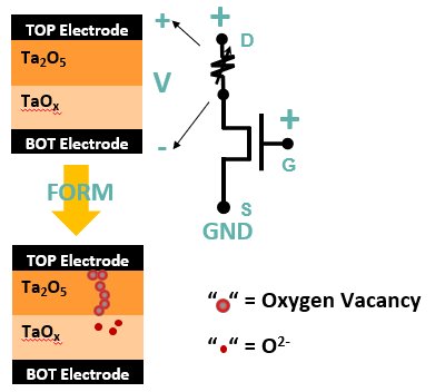
Fig. 2a, FORMing of an RSE
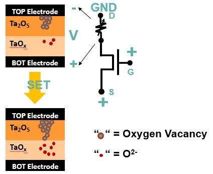
Fig. 2b, SET of an RSE
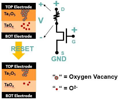
Fig. 2c, RESET of an RSE
Status
eMemory is releasing its first ReRAM IP on UMC’s 40nm ULP (ultra-low power) process this quarter (Q3/2021) and is currently developing 22nm’s version simultaneously. Below are the key features of the first IP on 40nm ULP. Aiming at code storage and lookup table in the first delivery stage, eMemory is still exploring the range of device operation and reliability trade-offs and may release an update in the near future.
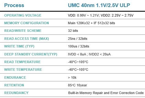
Tab. 1, Spec of eMemory’s first ReRAM IP
REFERENCES
[ref. 1] “Resistive Random Access Memory (RRAM): an Overview of Materials, Switching Mechanism, Performance, Multilevel Cell (mlc) Storage, Modeling, and Applications”, Furqan Zahoor et al, Nanoscale Research Letters, 2020
[ref. 2] “ReRAM technologies for embedded memory and further applications”, Satoru Ito et al, International Memory Workshop, 2018
[ref. 3] “Oxygen vacancies: The (in)visible friend of oxide electronics”, Felix Gunkel et al, Applied Physics Letters, 2020
[ref. 4] “OFF State Conduction in Filamentary RRAM”, Dipesh Niraula et al, IEEE Electron Device Letters, 2019
Related Semiconductor IP
Related White Papers
- CFET Beyond 3 nm: SRAM Reliability under Design-Time and Run-Time Variability
- Intellectual-property vendors look beyond RTL
- 'Smart' verification moves beyond SystemVerilog 3.0
- Taking on the 130nm node and beyond
Latest White Papers
- ACE: Confidential Computing for Embedded RISC-V Systems
- Customizing a Large Language Model for VHDL Design of High-Performance Microprocessors
- CFET Beyond 3 nm: SRAM Reliability under Design-Time and Run-Time Variability
- Boosting RISC-V SoC performance for AI and ML applications
- e-GPU: An Open-Source and Configurable RISC-V Graphic Processing Unit for TinyAI Applications