DDR SDRAM Controller IP Designed for Reuse
Federal University of Rio Grande do Sul
Porto Alegre, Brazil
Abstract :
This paper deals with reusability issues in the development of a double data rate (DDR) SDRAM controller module for FPGA-based systems. The development of integrated systems-on-a-chip (SoC) is based on the reuse of modules, or intellectual property (IP) cores. Moreover, the development and validation time of very complex systems can be reduced with the use of high level description and rapid prototyping by integrating modules into a FPGA device. Nevertheless, delay sensitive circuits like DDR memory controllers not always can be fully described by using a generic reusable code language. With our approach, it is possible to generate a highly reconfigurable DDR controller that minimizes the recoding effort for hardware development.
1. INTRODUCTION
Systems-on-a-chip can integrate different hardware elements as processors and communication modules over the same chip. Each hardware element is a closed block defined as an intellectual property (IP) module. The reuse of IP modules in the construction of different SoCs is a fast way to reach system integration. New generation high-performance and high-density FPGAs become prototyping devices suitable for verification of SoC designs. However, only few megabytes of memory are available inside FPGA devices and an external memory is needed if the application handles large amounts of data.
In this scenario, double data rate synchronous RAM (DDR SDRAM) has as main characteristics large capacity to store data, low cost and high bandwidth. An external memory controller (EMC) module is used into the SoC to interface with the DDR memory.
Memory devices, either used as single elements or as dual-in-line memory modules (DIMM), have standardized interfaces. Thus, the EMC design targets a reusable IP module shaped to the system needs. At this point, the use of a hardware description language (HDL) as Verilog or VHDL adds some benefits to the design as it:
- Uses high-level system description allowing human readable codes;
- Is a technology-independent system description that can be reused with a minimum of recoding, provided if logic elements are not instantiated from libraries;
- Allows design verification by high-level simulation before the gate-level implementation.
However, as the HDL code was not originally intended as an input to generate hardware, many language constructions are not supported by the synthesis software. The synthesis tools use different language subsets to translate the description code to logic elements. The hardware designer must use coding strategies to create a source code that can be synthesized. The understanding of the synthesis tool process and the knowledge of the FPGA features are important to design the hardware module. Also, the hardware developer must to know the placement and timing parameters to reach the system specifications.
As is proposed in the reuse methodology manual [1], the IP module design flow can be structured in five steps before its implementation and test in the development board (Fig. 1): 1) system requirements definition and module technical specifications; 2) design conception, test bench and timing specifications; 3) HDL design-entry description; 4) logic synthesis and; 5) Physical implementation.
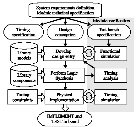
Fig. 1: IP module design flow for FPGA
The design-entry is structured using the language subsets for the synthesis tool, after the system requirements and module technical specification step. It can be structural (topologically-defined), instantiating pre-defined blocks from vendor library models into the code; or behavioral, describing the module functionality in a high-level of abstraction. In the logic synthesis step, the design-entry is translated into hardware logic elements by inference or using the vendor library models. The final step before the system prototyping is the physical implementation. In this step, the components instantiated in the code are mapped from the vendor library and the timing constraints are used to implement the module. In parallel with the design flow, each module development step is accompanied by a stage of verification: the functional simulation of the HDL code; the timing analysis of the module logic synthesis and; the timing simulation of the module physical implementation.
The DDR SDRAM controller uses architecture specific primitives and macros that are instantiated in the HDL code using the vendor library models. A synthesis tool is not able to translate these specific macros in the design-entry by inference. Then, some recoding effort is necessary when reusing the controller IP on a different platform. Such features characterize a firm-IP module, which targets a specific architecture and has a higher level of optimization. Firm cores are traditionally less portable than soft cores, but have higher performance and more efficient resources utilization because they are optimally mapped, placed and routed. Moreover, optimization or unconstrained routing by synthesis and routing software may change critical timing relations for correct hardware behavior.
In this paper it will be presented an architectural description of the DDR memory controller for FPGA implementation. Also, it will be presented the DDR controller components that are technology-dependent and the FPGA fabric solutions from Xilinx and Altera manufacturers. At the end of the paper it will be reported the implementation results on a Xilinx Virtex-2 Pro device interfacing with a DIMM DDR SDRAM.
This paper is organized as follows: section 2 presents an overview of the DDR memory and controller; section 3 shows the controller technology-dependent components; section 4 presents the implementation and validation steps and in section 5 the conclusions are discussed.
2. DDR SDRAM CONTROLLER IP
In this section it will be introduced the main characteristics of DDR memory and controller.
Double data rate memories contain three buses: a data bus, an address and a command bus. The command bus is formed by the signals column-address strobe (CAS), row-address strobe (RAS), write enable (WE), clock enable (CKE) and chip-select (CS). The data bus contains the data signals (DQ), data mask (DM) and data strobe signals (DQS). Address bus is formed by address (ADDR) and bank address (BA) signals. These memories operate with differential clocks CK and CKn, which provides source-synchronous data capture at twice the clock frequency. Data is registered either in the rising edge of CK and CKn. The memory is command activated starting a new operation after receive a command from the controller.
Data words are stored in the DDR memory organized in banks, indexed with row, column and bank addresses. Fig. 2 illustrates the timing diagram for a RD operation in DDR memory. Data is transferred in bursts, sending or receiving 2, 4 or 8 data words in each memory access.
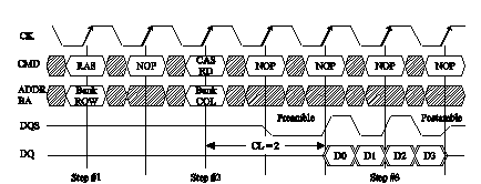
Fig. 2: Timing diagram of reading data from DDR memory with CAS latency 2 and burst length 4.
To access data in a read (RD) or write (WR) operation, the controller first sets the row address, this is called as row-address strobe (RAS) command (Step #1). After, the memory controller sets the column address, called as a column-address strobe (CAS) command (Step #2). In the case of a RD operation, data is available after the CAS Latency (CL) which can be 2, 2.5 or 3 clock cycles (Step #3). The data words D0:D3 are transmitted edge aligned with the strobe signal DQS after the CAS latency. DQS is a bidirectional strobe signal used to capture data DQ.
Dynamic memories, as the DDR SDRAM, require refreshing the stored internal data periodically. This operation is performed by the memory controller using the auto-refresh command.
2.1. DDR Controller Clock Generation
The traditional synchronous and skewless clock network distribution schemes are not feasible in DDR SDRAM memories. In order to interface with this type of memories, data is transmitted simultaneously with a non-free running clock.
The memory controller IP uses more than one clock for exchange command and data with the external memory. Two data words are transferred in one clock cycle in DDR memories. This suggest a FPGA implementation of the memory controller IP that uses one clock to capture first data word and other clock shifted by 180 degrees to capture second data word. The data transferred is source synchronous, and the DDR uses the data strobe signal DQS to Read and Write data operations.
All clock signals used by the controller to capture data send from external memory are generated by local inversion. The FPGA must provide to the controller apart from the system clock (CK), a 90 degrees shifted clock. This is done by a clock manager module, as a phase-locked loop (PLL), internally or externally to the FPGA. Local clock inversion in the registers is used to generate CK180 and CK270. Command and address are sent to memory in the rising edge of CK180, at single data rates. However, data are sent to external memory using both CK90 and CK270.
The clock generation is a technology dependent resource and each FPGA manufacturer use different embedded modules to make internal clock management. Also, best design practices recommend that the clock generation and control has to be done externally to the DDR controller, in a separated module. Each system implementation must generate suitable clock and reset signals to the controller, in conformance with the external memory frequency.
2.2. Read data capture using DQS
The most challenging task in interfacing with DDR memories is to capture read data. Data transmitted by DDR memory are edge aligned with the strobe signal, as is illustrated in Fig. 2. The controller uses both strobe signal transitions to capture data, rising and falling. The strobe signal must be delayed 90 degrees with respect to DQ to be aligned with the center of data valid window.
In Fig. 3 is illustrated the circuit topology used to capture the data read from DDR memory. A Delay Line is inserted into the DQS path in order to shift the strobe signal by 90 degrees, as described in [2].
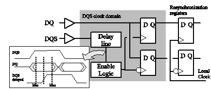
Fig. 3: Circuit topology to capture the data read.
The DQS strobe timing pattern consists of a preamble, toggling and postamble portion, as illustrated in Fig. 2. The preamble portion provides a timing window for the receiving device to enable its data capture circuitry. The toggling portion is used as clock signal to register data using both strobe edges. The amount of delay between data and strobe signals has to satisfy minimum and maximum values to successfully capture data send by the external memory device. In the implementation step, the data and strobe delays are controlled not only by the delay-line size but also by the internal routing delay.
The Enable Logic is used in the data capture circuit to avoid false triggers of the capture circuit. Following the preamble, the strobes will toggle at the same frequency as the clock signal for the duration of the data burst. D-type registers synchronized with the delayed strobe signal are used to capture read data from memory.
2.3. DDR controller architecture
The DDR controller contains the logic used to control data accesses and the physical elements used to interface with the external memory. Its design objectives the creation of a configurable IP module, to be used into different SoC designs, allowing the configuration of: DQ data bus width and the number of DQS strobes; the data burst length; the CAS latency; the number of clock pairs, chip-select and clock-enable signals to memory.
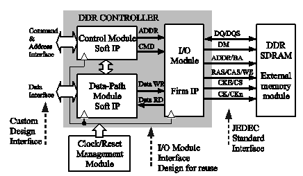
Fig. 4: DDR controller block diagram.
The DDR controller architecture is structured in three sub-blocks, as illustrates Fig. 4:
Control module – controls the data access operations to external memory translating the user commands and addresses to the external memory. Also it controls the write and read cycles and the data maintenance generating the auto-refresh command periodically. It is implemented as a soft-IP module described in HDL;
Data-path module – data sent and received from DDR memory are processed by this module. In transmission, data are synchronized using the double data rate registers. In reception, data are stored into internal FIFOs and it is synchronized by the controller internal clock. It is implemented as a soft-IP module described in HDL;
I/O module – contains the I/O and 3-state buffers located at the FPGA IOBs device and the double data rate registers used to write and read data, commands and to generate the clock signals to memory. It is a firm-IP module described in HDL with pre-defined cell and I/O location.
In Fig. 5 is illustrated a simplified block diagram of the I/O module that interfaces with external SDRAM memory. This module contains the technology-dependent elements like the DDR registers, SSTL drivers and the delay-lines. The signals used to control the interface as the addresses and commands are sampled by D type registers. The data and mask signals are sampled using DDR registers with clock inputs synchronized by CK90 and CK270 in the writing and by DQS Read in reading. Also, the control interface generates DQS Control signal to tune the delay-line at the data capture.
In the next section, a comparison between the different technologies used by Altera and Xilinx to implement DDR controllers is presented.
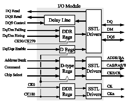
Fig. 5: DDR controller I/O Module block diagram.
3. TECHNOLOGY-DEPENDENT ELEMENTS
The FPGAs from Xilinx and Altera use different embedded features to implement DDR controllers. Information presented below was obtained from Altera’s MegaCore user guide [3], Xilinx application note [4] and libraries guide [5].
SSTL-2 signaling – the normal drive strength for all inputs and outputs is specified as SSTL-2, defined in the JEDEC Standard [6]. This feature is present in Xilinx’s Spartan-3, Virtex-2, 2P, 4 and 5 and Altera’s Stratix and Cyclone device families. The drives strength must be specified by the system designer in order to correctly perform design prototyping.
Frequency shift – circuit used to generate the 90 degrees phase clock. Both Altera’s Stratix and Cyclone families contain the Enhanced phase-locked loop that provides phase shifting. The Spartan-3 and Virtex-2, 2P, 4 and 5 families contain Digital Clock Managers (DCM) elements.
Double data rate registers – used to send and receive data to external memory. Altera’s Stratix family contains dedicated DDR registers called DDIO built in the I/O element (IOE). In Cyclone series, the DDR input registers are implemented with three internal logic elements registers (LE). These elements are used by primitive instantiation in the HDL code. For Xilinx’ Spartan-3, Virtex-2, 2P, 4 and 5 device families, built-in DDR input and output registers are available at the I/O blocks. For Xilinx’ Spartan-3, Virtex-2, Virtex-2 Pro and Virtex-4 device families, input DDR registers are inferred by the Xilinx ISE tool. Output DDR registers must be instantiated using FDDRRSE, FDDRCPE or ODDR (Virtex-4,5) primitives.
DQS delay circuit – used to center-align the data strobe DQS with data DQ. In Altera’s Stratix and Stratix-II devices series, the input-output element (IOE) provide a process, voltage and temperature (PVT) dynamically compensated 90 degrees phase shift to delay DQS. In Stratix-III and IV, a DQS phase-shift circuitry uses a DDL to capture read data. In Cyclone series, the phase shift is guaranteed by manual instantiation of LEs forming static delay chains. The value of the delay is set by a constraints script used in the implementation design step. For Xilinx’ Virtex-4 and Virtex-5 devices families, absolute delay elements called IDELAY provide picoseconds resolution over PVT. They are built into each IO block and are used to configure the delay over the DQS group. In Spartan-3, Virtex-2 and 2P device families, the delay is built with a chain of internal logic elements (look up tables or LUTs). The amount of delay is controlled by the number of LUTs inserted in the DQS signal. All resources listed before must be instantiated in the HDL code by the module developer from the correct vendor library. In our approach, these resources are grouped together into the I/O sub-block in order to increase the design reusability by facilitating the recoding process.
The design-entry recoding to adapt the controller to another board begins with changing de signals interface width, through the definitions declared with generics at the top-level entity. The I/O module signals, detailed in Fig.5, are automatically fit in wide. Internal logic elements instantiated in the code as the Delay Line, the DDR registers and the STLL drivers, are manually replaced by the user.
4. IMPLEMENTATION AND TESTS
The DDR memory controller can only be considered validated after its successful operation on an actual circuit. The physical implementation results and the system prototyping procedure are presented in this section.
4.1. Controller Implementation
The DDR controller was implemented in VHDL language, structured into sub-blocks as showed in section 2. The I/O module was implemented in structural format as a firm-IP by instantiating individually defined technology-dependent elements from the Xilinx Unisim library. It contains SSTL driver buffers, the DDR registers and the logic elements used to implement the delay line circuit. Also, the clock generation circuit is realized by instantiating one DCM from the Unisim library in the VHDL code, on a module separated from the DDR controller IP.
The Digilent XUPV2P board is used as system platform to test the DDR controller. This board contains a Virtex-2 Pro FPGA with a 100 MHz clock oscillator and external 512 MB DIMM DDR SDRAM module.
Before the board implementation, both functional and timing simulations were performed using Modelsim XE 6.0a software. The synthesis results for a XC2VP30 Virtex-2 Pro FPGA using ISE WebPack 10.1 tool are shown in the Table 1. The controller was implemented for DQ 64-bit wide, DQS 8-bits wide and achieves frequencies higher than 220 MHz.
Table 1: DDR controller synthesis results.
| Sub-block | Slices | flip-flops | LUTs | # lines |
| Control | 156 | 187 | 268 | 1559 |
| Data-path | 802 | 931 | 755 | 981 |
| I/O | 67 | 180 | 134 | 824 |
| DDR controller | 580 | 1299 | 1135 | 4111 |
As a measure of the reusability of the code, one can count the number of lines that the designer can keep from a design to the next one. The recoding effort in adapting the DDR controller to a new design is done over about 20% of the total source code lines, disregarding the clock generation module. The controller’s soft sub-blocks are the control and the data-path and the firm sub-block is the I/O, which represents 11% of all the slices used by the controller. The synthesis results show that the reusable code part is most significant in this design.
After the synthesis, the next step in the design flow is the physical implementation in the FPGA. ISE tool performs the physical implementation from three processes: translate, map and place&route. In this last step, the timing and placement constraints defined by the developer are used. The placement constraints allow the tool to map the controller to the FPGA pins that interface the external memory.
The synthesis tool uses the timing constraints to force the routing step to meet the system timing requirements for the FPGA implementation. Also, they are used to set the system clock speed and the maximum allowed delay in specific nets. In the DDR controller implementation, the constrained nets are the DQS delayed used as clock to capture read data. In the ISE tool, the maximum delay allowed to a given net is set in the user constraints file (UCF) by the line:
NET "net_name" MAXDELAY = 2500ps;
Existent constraints for implements the controller technology-dependent elements can be reused without recoding in different designs. If the user chooses another synthesis tool to implement the controller, the constraints file must be modified.
4.2. Test and Verification
The DDR controller verification is complete after the test over the development board. Both functional and timing simulations are not enough because they do not take into account the external propagation delays. Also, memory modules can present skew between data and strobe signals, generating an unpredictable data capture behavior.
In the controller side, all data signals can only be captured via a DQS edge send by the external memory, during a given time window, known as the data valid window (DV). DV window depends on both the memory device and controller setup and hold times, the duty cycle distortion, the package skew and on main board routing delay due to track impedance from memory to FPGA device.
Memory test methods can be used to detect timing spreading generated by FPGA internal or external routing delays. The test approach uses the DDR controller IP, the interconnections between memory and FPGA and the external memory as a single circuit under test. Supposing that the external DDR SDRAM memory is free from errors, writing a data pattern into the external memory and reading it back is used to validate the DDR controller implementation.
A built-in self-test module is used to generate the data pattern applied to the DDR controller, selecting the memory operation, address range tested and the data pattern. The test methodology used to verify the DDR controller was already presented in [7].
5. CONCLUSIONS
Complex systems that use large amounts of information, as the multimedia equipments, need external memory modules to hold temporary data. The use of FPGAs for system prototyping and verification is interesting but they have limited internal memory capacity. DDR memories are very efficient devices but the design of FGPA DDR memory controllers is a challenging task. This paper presented reusable IP module with minimum non recurrent engineering effort by structuring the design.
The main purpose in using a hardware description language, beyond system simulation and verification, is to reuse the code in different system implementations. When dedicated logic elements are used to interface with the external DDR memory, it is necessary to instantiate some elements from vendor libraries at defined device locations. These circuits are isolated into firm modules and are reengineered for each new device or circuit board. The controller logic and state machines are encapsulated on soft modules and reused as-it-is into new designs. Also, as we have presented in this paper, the knowledge of the limitations of the synthesis tool is important to guide the implementation in order to meet the design requirements.
The integration of a BIST module with the controller is very useful to allow automatic test of the IP implementation when reusing it in other systems. The test approach uses the DDR controller IP, the interconnections between memory and FPGA and the external memory as a single circuit under test.
In the last years, the new FPGA devices started to port new embedded elements to support faster double data rate memory interfaces standards like DDR2 and DDR3. The use of these elements in new memory controllers, however need a design methodology like the one presented in this paper.
REFERENCES
[1] M. Keating and P. Bricaud, Reuse methodology manual: for system-on-a-chip designs. Norwell, MA, USA: Kluwer Academic Publishers, 1998.
[2] K. Ryan, “DDR SDRAM functionality and controller read data capture,” Micron Design Line, vol. 8, p. 24, 1999.
[3] MegaCore: DDR and DDR2 SDRAM High-Performance Controller User Guide, Altera Corporation, 2008.
[4] Application Note 802: Memory Interface Application Notes Overview, Xilinx, 2007.
[5] ISE 8.1i Software Manual: Libraries Guide, Xilinx, 2007.
[6] JEDEC, JESD79: Double Data Rate (DDR) SDRAM Specification, JEDEC Solid State Technology Association, Virginia, USA, 2003.
[7] A. C. Bonatto, A. B. Soares, and A. A. Susin, “DDR SDRAM Memory Controller Validation for FPGA Synthesis,” in LATW2008: Proceedings of the 9th IEEE Latin-American Test Workshop, Puebla, Mexico, Feb. 2008, pp. 177–182.
Related Semiconductor IP
- DDR SDRAM Controller
- AMBA AHB Bus to DDR SDRAM Controller
- DDR SDRAM Controller - Pipelined for ispXPGA and ORCA4
- DDR SDRAM Controller - Non-Pipelined
- DDR SDRAM Controller - Pipelined
Related White Papers
- The Love/Hate Relationship with DDR SDRAM Controllers
- Designing DDR3 SDRAM controllers with today's FPGAs
- Transactional Level Modeling (TLM) of a High-performance OCP Multi-channel SDRAM Memory Controller
- Implementing custom DDR and DDR2 SDRAM external memory interfaces in FPGAs (part 1)
Latest White Papers
- How Next-Gen Chips Are Unlocking RISC-V’s Customization Advantage
- Efficient Hardware-Assisted Heap Memory Safety for Embedded RISC-V Systems
- Automatically Retargeting Hardware and Code Generation for RISC-V Custom Instructions
- How Mature-Technology ASICs Can Give You the Edge
- Exploring the Latest Innovations in MIPI D-PHY and MIPI C-PHY