Clock Mesh Variation Robustness: Benefits and Analysis
Circuit delay is increasingly affected by process variations at lower technology nodes. Global variations are in double digits now, and according to the International Technology Roadmap for Semiconductors (ITRS) the trend is rising. Variations in the manufacturing process may cause two gates that are electrically identical and in close proximity to significantly vary in delay. Consequently, designers add significant timing margin to safeguard their designs against timing violations.
Technologies that offer variation tolerance boost design performance and productivity. Clock mesh technology provides uniform, low skew clock distribution and offers better tolerance to on-chip variations (OCV) than conventional clock tree technology. The need to control OCV effects is now driving clock mesh technology to mainstream designs.
This article gives an overview and highlights the benefits of clock mesh technology compared to conventional clock tree methods.
Clock Mesh Robustness Minimizes OCV Effects
Variation at Advanced Technology Nodes
There are two source classes of variation that must be considered in design, global and local. Global chip-to-chip variations cause performance differences among dies and are modeled as operating corners. Local on-chip variations cause performance differences among transistors within the same die and are modeled as an added derating factor to skew calculations. What are the specific causes of these local variations?
Transistors located in close proximity on the same chip exhibit variation in their characteristics due to random manufacturing variations in:
- the number and location of doping atoms
- the length and width of the transistor channel
- the thickness of oxide layers across the die
Timing derating is the universally accepted method to model the maximum OCV that the design is expected to incur. Newer technology nodes feature increased gate speeds as well as increased susceptibility to variation. Because of this, the derating factor has also
increased, and today it is common to see derating between 5 percent and 10 percent. Thus, it becomes necessary to design circuit structures that are inherently variation tolerant to reduce the adverse impact of OCV derating.
Clock mesh is a clocking scheme employed by high-performance design teams to achieve low skew and high OCV tolerance. The large impact of OCV derating on conventional clock trees motivates mainstream design groups to also consider clock mesh. An examination of clocking structures explains why.
Clock Mesh versus Conventional Clock Tree Structure
The structures of a conventional clock tree and a clock mesh are shown in figure 1. The clock tree has a clock source, clock tree cells, clock gating cells and buffers and loads. The clock mesh includes a clock source, pre-mesh drivers, mesh drivers, the mesh net, clock gates and mesh receivers, and loads.
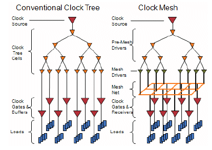
Figure 1: Clock Structures - Conventional clock tree and clock mesh
The main difference is the presence of the mesh net. Another major difference is that the mesh drivers are connected to the mesh net as a multi-driven net. Clock mesh implementation requires an array of mesh drivers, shown in green in figure 1, to drive the massive RC network of the clock mesh.
The benefit of the mesh net is that it smoothes out the arrival time differences from the multiple mesh drivers that drive it. The smoothing effect of the mesh net is visualized with circuit simulation of an actual test case shown in Figure 2. The top trace is the ideal clock, the top pair of traces shows the skew just before the mesh, and the bottom pair of traces shows the skew just after the mesh.
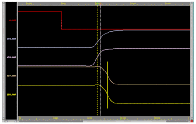
Figure 2: SPICE waveforms showing the smoothing effect of the mesh net
These timing waveforms show that the mesh receivers are switching in a very narrow timing window compared to the mesh drivers. In the analysis section, Monte Carlo simulation is used to validate over randomly varied conditions showing that the range of skews at the output of the mesh is narrow compared to the range at the input of the mesh.
Table 1 lists the skew data for two test cases. Even before considering OCV derating, the clock mesh versions of the designs are clearly superior in terms of skew performance.
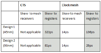
Table 1: Insertion delay and skew of clock tree and clock mesh
Understanding OCV Derating
For the majority of loads in a clock tree design, very little of the overall path back to the clock root is shared. The converse is true for a clock mesh design where the path from the clock root to the mesh net is shared by all loads. Thus only the paths from the mesh net through the clock gates and receivers to the loads are adversely impacted by variation effects. The variation above the mesh net is negligible.
OCV derating values range from 5 percent to 10 percent depending on the technology node and design knowledge. A typical derating factor is 7 percent. Thus, for setup-checks, the non-shared launch path is increased by 7 percent, and the non-shared capture path is reduced by 7 percent. In Figure 3, the skew is assumed to be 2 percent of the total insertion delay for both design styles. This is unlikely to occur in practice since clock mesh designs yield much better skew, but holding skew constant highlights the impact of OCV derating. Even this unrealistically conservative example shows that clock mesh has almost four times better OCV tolerance.
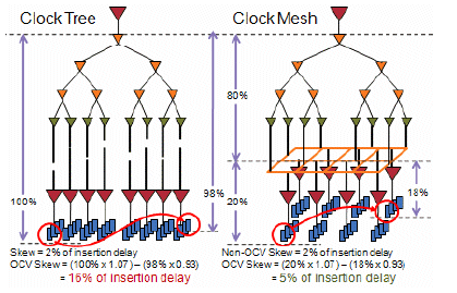
Figure 3: OCV tolerance - clock tree vs clock mesh
Since OCV derating only occurs between the unique portions of the launch and capture paths, the benefit of clock mesh OCV immunity is significant - in this example four times better. Per ITRS variation effects increase as feature sizes decrease. As the adverse impact of OCV continues to increase, the benefits of clock mesh over clock tree become even more pronounced.
Design and Analysis of a Clock Mesh
Mesh Fabric Design
Mesh fabric design is critical to achieving a balance of skew performance and design resource conservation. The parameters that have the greatest impact are the mesh spine width and pitch.
Circuit simulation analysis verifies that as the mesh spine width increases, the skew to the mesh receivers decreases. But when the mesh spine width increases beyond the drive capacity of the mesh drivers, the trend reverses and the skew increases.
Analysis also determines the result of different mesh spine pitches, from 100 microns x 100 microns to 150 microns x 150 microns. As the pitch increases so do the routing resources. Unfortunately skew also increases. The wider mesh pitch induces longer routes from the mesh net to the mesh receivers, which degrades skew and OCV tolerance.
After the mesh net topology has been analyzed and validated, it is time to evaluate the OCV performance of the entire clock design.
Simulation and Analysis of OCV Effects
Monte Carlo simulation is a method of applying random variations to simulate the manufacturing process. Varying the SPICE “lint” parameter of the NMOS/PMOS transistor model emulates the random variation of doping atom deposition in the transistor’s channel. During the Monte Carlo simulation, a different random value is produced for each transistor in the netlist. A Gaussian variation with zero mean and a sigma equal to 5e-9 is modeled. The “lint” parameter is varied in the range from -4 to +4 sigma, (-20nm to +20nm). Thus if the drawn length is 90nm, and the nominal lint is 0, the effective length of the device varies between 50nm and 130nm.
Figure 6 shows the results of a Monte Carlo simulation over 30 iterations. The skew variations at the receiver inputs, shown in blue, demonstrate a very small skew variation from the clock source to the mesh receivers.
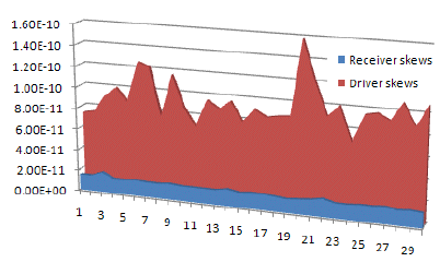
Figure 4: Monte Carlo simulation results varying the "lint" parameter
The results shown in red are the skew variations at the mesh driver input pins. The skew variations before the mesh net are extremely large (60ps to 160ps), but the skew variations after the mesh net (14ps to 16ps) are small and validate that the multi-driven mesh net equalizes the delay.
Circuit simulation testing determines the optimum mesh spine width and pitch for a given drive capability. Monte Carlo SPICE simulation testing validates that the clock mesh produces low clock skew and has a strong immunity to on-chip variation.
Conclusion
At advanced technology nodes, the manufacturing process exhibits multiple sources of OCV effects. Timing derating factors guard against OCV effects but at a significant cost when using conventional clock tree technology.
Clock mesh technology produces a much lower clock skew compared to a conventional clock tree and, more importantly, is inherently OCV tolerant. OCV derated clock mesh designs generally have both lower skew and higher performance than clock tree designs.
Circuit simulation testing is used to both determine optimum design parameters as well as to validate the performance of clock mesh designs.
References
1. Process Variability at the 65nm node and Beyond – Sani.R.Nassif IEEE 2008 CICC.
2. The International technology Roadmap for Semiconductors, 2007.
Mallik Devulapalli is staff engineer in the strategic partnership CAE group at Synopsys. He holds a master's degree in telecommunications management from California State University, Hayward. His recent works include high-performance and low-power methodology development for 45nm technology for a Synopsys partner.
Yuichi Kawahara is senior staff corporate applications engineer. His recent work includes high-performance and ultra low-power chip methodology development, working with a Synopsys partner. He studied computer information science at Temple University in Philadelphia and holds an MBA from Marylhurst University in Portland, Oregon.
Related Semiconductor IP
- NPU IP Core for Mobile
- NPU IP Core for Edge
- Specialized Video Processing NPU IP
- HYPERBUS™ Memory Controller
- AV1 Video Encoder IP
Related White Papers
- Power analysis of clock gating at RTL
- Synthesis-aware clock analysis and constraints generation
- SoC clock monitoring issues: Scenarios and root cause analysis
- Reducing false errors in clock-domain crossing analysis
Latest White Papers
- Breaking the Memory Bandwidth Boundary. GDDR7 IP Design Challenges & Solutions
- Automating NoC Design to Tackle Rising SoC Complexity
- Memory Prefetching Evaluation of Scientific Applications on a Modern HPC Arm-Based Processor
- Nine Compelling Reasons Why Menta eFPGA Is Essential for Achieving True Crypto Agility in Your ASIC or SoC
- CSR Management: Life Beyond Spreadsheets