Behavior Analysis for SoC Debugging
Novas Software, Inc.
ABSTRACT
In this paper, we present a behavior analysis technique for hardware debugging of complex System-on-Chip (SoC) designs. As designs get more and more complex, there is a need to analyze the design behavior in order to accelerate designer understanding of its behavior. Our behavior analysis technique delivers significant technology advances in debugging; it is the first approach of its kind that extracts, analyses, visualizes, and empowers exploration of a design’s multi-cycle temporal behavior. This new technology significantly shortens debugging time and reduces the number of regression iterations.
INTRODUCTION
Architecting today’s large and complex SoC designs is a major undertaking because these designs typically exhibit the following characteristics, each with its own set of debug challenges:
- In addition to internally developed functions, the designs contain Intellectual Property (IP) components from multiple third-party providers. Understanding the way in which these IP components function in the context of the system can be extremely demanding.
- Throughout much of the system design process, components are represented using mixed levels of abstraction ranging from behavioral, Register Transfer (RT), to structural gate levels. Debugging designs represented at multiple levels of abstraction is non-trivial.
- The simulation stimulus and response data used to exercise these designs and observe their behavior can be huge. Analyzing this data and correlating the expected (desired) behavior with the actual (implementation) behavior is a mammoth task.
The ability of design and verification engineers to understand intricate and unfamiliar designs is crucial to the successful completion of design projects. Poor understanding leads to long integration and debug cycles, slipped schedules, and invariably increased project cost.
In IC design, the terms “verification” and “debug” are used interchangeably. We, however, would like to make a distinction between the two. The verification process consists of two complimentary yet dissimilar components, which we can call detection and debug.
Detection uses simulators, testbench tools, and formal tools to determine whether errors are present. Since it is all but impossible to know when “enough” verification has been done, detection tools are deployed in vast numbers to exercise the design as much as possible in the time available. Detection can be accelerated by running batteries of tests in parallel on many computers simultaneously.
Debug is quite different. It cannot be run in the background on banks of servers because it requires the direct, continuous involvement of an engineer. In this part of verification, engineers track down the root causes of errors detected by the other tools. The process of debugging involves locating the logic that is associated with an error, isolating the pertinent cause and effect relationships, and understanding exactly how the design is supposed to behave and why it is not behaving that way. This process cannot be run in the background. It can only be accelerated by improving engineers’ ability to understand causes and effects within their designs.
Historically, detection has received more attention, but as designs get more elaborate we see that the tide is turning. Debug is no longer an afterthought; determining the cause of a bug is not obvious, correcting it is not a simple tweak. On the contrary, debug, with its demand on expert designer’s time and energy, is quickly becoming the bottleneck in the verification process. The fundamental idea in debugging is to comprehend the design’s operation i.e. its behavior over time. It is this (fast) comprehension that allows (quick) bug cause determination and correction. Debug therefore requires exploring the design in many different ways in order to fully understand it. In the rest of the paper, we first set the foundation by reviewing the historic evolution of debug approaches. We then briefly review current day techniques setting the stage for behavior based debug, detailed in the sections that follow.
EVOLUTION OF HARDWARE DEBUG
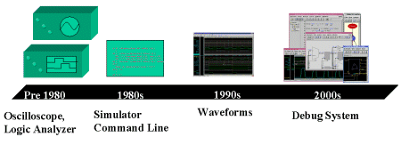
In the early days of digital design, before simulation software was widely used, the main debug tool was the oscilloscope. This analogue tool allowed engineers to probe one or two signals on a physical prototype. As digital technology advanced the logic analyzer emerged, allowing engineers to probe and view many more signals, and to record the history of the values for these signals. You might say that the logic analyzer is the direct ancestor of the waveform tools that have become the mainstay of simulation-oriented debug.
In the late 1980s, software-based logic simulation took hold as a replacement for physical breadboard prototypes. This gave engineers enormous flexibility in creating models with which to evaluate designs. But something was also lost in the evolution. The early simulators didn’t start out with waveform displays, so engineers had to look at tabular data showing signal values over time. However, as graphical workstations became more widely available, simulator user interfaces, which had been strictly command-line based, became more graphical. Waveform displays were the first big advance in simulation-based debug. Later, cross-probing between schematics and waveforms was introduced for gate-level designs, and then source code viewing was added with the rise of RTL design and synthesis. Each of these advances in debug technology reduced the time and effort required to track down the reasons for bugs detected by simulation. This is shown graphically in Figure 1 below.

Figure 1: Evolution of Hardware Debug
All popular simulation tools now come with basic graphical user interfaces built around waveform tools. These are adequate for simple designs and small design teams. However, these waveform tools, each with its own dedicated user interface, are limited by their reliance on proprietary simulator data structures, and do not provide a wide variety of ways to examine a design.
As time and design size marched on through the close of the 20th century, the need for better ways to explore complex designs drove development of independent comprehensive debugging tools, including the complete debug system pioneered by Novas [2]. These tools extract and store structural information from design sources and from detection tools, and provide convenient ways to traverse the stored connections.
TODAY’S DEBUGGING – STRUCTURAL ANALYSIS
Today’s debugging tools rely on structural information such as design connectivity using schematic and value change information from simulation result. When organized properly, rapid access to this structural information is highly valuable for accelerating debug.
As they explore a design to figure out how it works or why it does not, engineers are really trying to understand the dynamic behavior of the design. Ready access to the structure of the design and the results of detection tools gives them ways to speculate about the behavior – “if this is connected to that, then the design flow must be like so…” However, this approach relies entirely on the engineer’s ability to deduce the design’s behavior from its structure. No matter how well the structure is revealed, time is wasted making the wrong assumptions and following false paths. The more unfamiliar the design, the greater the difficulty and the more time required to reach adequate understanding. Engineers unfamiliar with portions of a design owing to design reuse, purchased IP, or diverse/dispersed design teams struggle to grasp how the design is supposed to work, or why it does not, leading to long integration and debug cycles.
By storing, organizing, and making information accessible, this structural approach has greatly accelerated design exploration and debugging. However, looking forward, as designs become more complex, debugging approaches must keep track and not lag behind; it is clear that even more power is needed. Design (debug) productivity will depend on more sophisticated approaches that automate more of the exploration and debug process and remove the mental burden of surmising (incorrectly) about the design’s behavior over time. Further advances in design exploration productivity must come from application of advanced technologies such as those that underlie synthesis, formal, and semi-formal verification tools (see [1] and [3]). A new behavior-based approach to debug is needed.
NEW TECHNOLOGY – BEHAVIOR BASED DEBUG
We present a new technology that performs rigorous mathematical analysis of a design to automatically infer its behavior and thus accelerate design understanding. This technique was first applied in synthesis tools and is being increasingly applied to functional verification detection tools.
We apply this technology to the design debugging sub-problems of design understanding, bug cause determination, and exploration. Key elements underlying our approach include:
- Behavior extraction: Given the source of an error, we automatically extract the temporal behavior of the design from the design logical model and the simulation data.
- Temporal Visualization: We provide new visual representations of the design that show its behavior unrolled over time in terms of data/control flow, and statement flow.
- What-if exploration: We provide dynamic exploration tools that allow engineers to run “what-if” scenarios with their designs by changing simulation values and even RTL statements and determining the consequences of those changes in order to understand the effect of alternatives before committing changes to the source files and re-simulating.
The sections that follow discuss these elements in more detail.
Behavior Extraction
Given an error source (e.g. signal value and time), we extract the temporal behavior that produces the error from the design HDL description and the simulation results. The extraction procedure is divided into two steps:
- Inference: This step converts an HDL description into a logic behavioral model. In other words, this step builds an internal model for the actual circuit logic operation. The control and data-path can be differentiated after this step.
- Temporal behavior expansion: Starting from any (user) chosen signal and time, we trace back through its (transitive) fanin cone to the register (or primary input) boundary, applying the clock timing to the fanin registers based on their associated clock signal and relative to the chosen signal’s (so-called reference) time. The values of signals are fetched from a simulation dump file or evaluated based on values already created in the debug system. The active and non-active elements in the fanin cone are also identified. This expansion can be performed interactively again and again moving backwards in time thus creating a temporal behavior representation that leads all the way back to the error source.
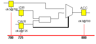
For example, let us assume we want to understand the cause of value 55 for signal ACC at time 800 in Figure 2. We first traverse the fanin cone of signal ACC backward until we hit the registers or input signals. Then, based on the clock signals of the registers and the simulation results, we can determine when each register was activated. For this example, the active fanins were ACC at time 700 and IDR at time 72. The control line is displayed prominently in the Figure.

Figure 2: Behavior Extraction
Temporal Visualization
During behavior debug, designers are able to incrementally build and analyze every additional sequential logic stage one at a time, determining which fanin signals they want to continue to trace. This continues until they find the cycle that is causing the error output. The tracing may cross multiple clock cycles boundaries, so the debugger must be able to handle this as well as present to the user in a visually notable fashion. We present two ways to keep track of the tracing backward through simulated time – the register flow graph and the statement flow graph.
The register flow graph renders a design’s behavior by showing only the relationship between each register and its fanins (registers and primary inputs). Users see the fanin and fanout relationship as a register-level abstraction; the combinational logic information is hidden for clarity.
The statement flow graph shows HDL statement-by-statement how a value is used and when it is assigned during simulation. The system differentiates datapath logic from the control signals. Users are given the option to prune out all non-active elements (for the given simulation data), so that they can focus on the active fanin signals. Users can choose to use the statement flow graph to traverse through registers, or use the two flow graph views: register, and statement, in an orthogonal fashion.
Both new design behavior illustration views are thoroughly linked with traditional source code, waveform, schematic, and finite state machine views. Users can drag and drop signals between the new abstractions and the detailed structural views to explore details of the causes of behavior revealed by the new design analysis, and operation depiction.
What-if Exploration
Quite often, designers need to explore potential bug fixes in order to accurately repair a design. Our system provides the means for users to assume a different value for a signal at a specific time and quickly determine the consequences of such a hypothetical change. We provide an evaluation procedure that propagates the value forward through the time-expanded representation to determine if, and how this change will affect the output i.e. whether the output obtains the desired value or not. We also provide an inverse evaluation—more appropriately called justification procedure to determine the set of signal changes that drive the output to the desired value. The advantage of what-if exploration is that it quickly increases designer’s confidence with a potential bug fix. The exploration operatess on the local expanded representation; users need not exit the debugger to redo the simulation, and start over.
THE ARCHITECTURE AND METHODOLOGY
The behavior analysis technology is built on top of a complete structural debug architecture, yielding an integrated system for both structural and behavior-based debugging.
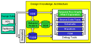
The structural analysis system consists of a database for structural design information, a database for simulation results, a waveform viewer, a schematic viewer, and a state diagram viewer. The expanded architecture adds a behavior database that stores the information needed to navigate the design behavior, and drive the temporal behavior illustration diagrams. The expanded debug architecture is shown in Figure 3 below.

Figure 3: The Expanded Architecture.
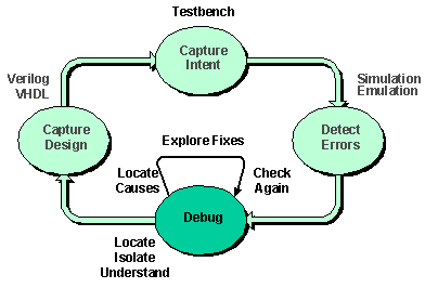
The architecture supports new tools that further accelerate the design and verification process. These new debuggers will help design teams reduce project costs, ensure their schedules, and avoid the risks associated with poor understanding and long debug cycles by locating causes of failures faster and exploring fixes locally during the debug process. The enhanced verification methodology is shown in Figure 4.

Figure 4: The Enhanced Verification Methodology.
EXPERIMENTAL RESULTS
With the behavior analysis technique, IC designers and verification engineers can quickly determine which design components are actually active during a selected span of simulation time. They can quickly trace the causes of values and assess alternative scenarios. They can use this capability to try out different combinations either to verify bug fixes or experiment with new test sets. Using this new technology, users report saving 30 to 60 percent of the time required to track down the causes of bugs in a variety of designs compared with the best structural tools.
CONCLUSIONS
We have presented a behavior-based debugging technique for SoC designs. Our debug approach [4] is divided into three major portions: behavior analysis, temporal visualization, and what-if exploration. The technique provides new abstractions that show a temporal overview of how a circuit works, and allow users to explore alternative behavior by experimenting with different input combinations without having to leave the debug environment. As designs continue to become more complex and involve larger numbers of design and verification engineers, the time savings and productivity enhancements provided by these new techniques will be invaluable.
REFERENCES
[1] Bertacco, Valeria, Maurizio Damiani, Stefano Quer: “Cycle-based Symbolic Simulation of Gate-level Synchronous Circuits”, DAC 1999, p. 392-396.
[2] Debussy, “Locate, Isolate, and Understand”, Novas Software, Inc., http://www.novas.com/products/debugDebussy.html
[3] Ganai, Malay; Aziz, Adnan; Kuehlmann Andreas, “Enhancing Simulation with BDDs and ATPG”, DAC 1999, p. 385-390.
[4] Verdi, “Behavior-Based Debug System”, Novas Software, Inc., http://www.novas.com/products/debugVerdi.html
Related Semiconductor IP
- DeWarp IP
- 6-bit, 12 GSPS Flash ADC - GlobalFoundries 22nm
- LunaNet AFS LDPC Encoder and Decoder IP Core
- ReRAM NVM in DB HiTek 130nm BCD
- UFS 5.0 Host Controller IP
Related Articles
- Simulating and debugging multicore behavior
- SoC clock monitoring issues: Scenarios and root cause analysis
- Analysis of RDC Paths for a million gate SoC
- ARM intrusive debugging for post-silicon SoC validation
Latest Articles
- VolTune: A Fine-Grained Runtime Voltage Control Architecture for FPGA Systems
- A Lightweight High-Throughput Collective-Capable NoC for Large-Scale ML Accelerators
- Quantifying Uncertainty in FMEDA Safety Metrics: An Error Propagation Approach for Enhanced ASIC Verification
- SoK: From Silicon to Netlist and Beyond Two Decades of Hardware Reverse Engineering Research
- An FPGA-Based SoC Architecture with a RISC-V Controller for Energy-Efficient Temporal-Coding Spiking Neural Networks