A Real-Time Image Processing with a Compact FPGA-Based Architecture
1Faculté des Sciences de Monastir
Avenue de l’Environnement 5019 Monastir - Tunisie
2Laboratoire ETIS, ENSEA Université Cergy Pontoise - France
Abstract
In this paper we present a filed programmable gate array implementation of a real time video smoothing algorithm. In comparison with smoothing video techniques like deblocking filters in H.264 or smoothing in JPEG2000, the proposed method is implemented in hardware and its computational cost and complexity are reduced. Our proposed architecture tries to optimize the design of a modified version of the Nagao filter in order to make video smoothing with respect to real time constraints. This filter have to smooth video before applying an edge extraction approach for manifacturing process control. The proposed architecture based on the RC1000P-P Virtex prototyping Board is analyzed to gain an understanding of the relationships between algorithmic features and implementation cost. Experimental results indicate that using this prototyping board with optimized hardware architecture; we can deliver real-time performances and an improvement in the video quality and deliver 30 images per second at 10 MHz clock cycle.
1. Introduction
With the growth of the heavy industries and the demand for high quality production, many industries such as plastics and textile industries require some form of technology for controlling their production quality. One common quality control technique employs cameras that capture the production activities for object dimension measurement with the assistance of an edge extraction algorithm [1]. In order to improve the edge detection technique we propose to smooth the video with a specific algorithm which operates in real time manner.
Furthermore, in image processing related to quality control applications where the inspection has to be accurate, it is difficult to analyze the information of an image directly from the gray-level intensity of the image pixels. Indeed, this value depends upon the lighting conditions. More important are the local variations of the image intensity. The size of the neighbourhood where the contrast is computed must be adapted to the size of the objects that we want to analyze (edge detection). This size defines a resolution reference for measuring the local variation of the image. Generally, the structures we want to recognize have very different sizes. Hence, it is not possible to define a priori an optimum resolution for analyzing an image. In this respect, we have to develop a smoothing technique in order to enhance the image contrast and to reduce noise. Consequently, this digital filter can be used in the pre-processing phase, as noise elimination, or in the enhancement of the edge detection.
This study have proposed a new smoothing technique that is implemented in only one FPGA-Virtex with additionnal memories. This technique consists in allowing on the central point with a neighbourhood 5x5, the sum of neighbourhood 3x3 among all with a minimal extent. The extent is defined as the difference between the Maximal and the minimal intensity related to contiguous pixels. In this context, we are particularly interested in addressing the results of the real time video smoothing based on the modified version of the Nagao algorithm, since it is used to improve the video quality by eliminating the noise inside the sequence. The other motivation is to present a generic methodology for rapid prototyping of a real time algorithm and shows how this compact hardware plateform is flexible enough to accurately support such complex applications having real time requirements. The video standards require the processing time less than 40 Ms per image (with a size of 5122) which indicates that a pixel must be computed each 100 ns taking into account the synchronization aspect. In this respect, the sampling frequency has to be about 10 MHz.
This paper is organized as follows: Section 2 relates to other works in this area. Section 3 willl describe the Nagamod algorithm and simplification hypothesis for a real-time hardware implementation. Section 4 presents the hardware implementation of the Nagamod filter. Section 5 is dedicated to experimental results. The results are presented in Section 6 where concluding remarks are given in Section 7.
2. Related Work
Smoothing is a technique of preprocessing which can be found in the segmentation chains [2] and in the compression of images. Indeed, the deblocking filter for example is used in the H.264/MPEG-4 video coding standard and carrying out simple operations in order to analyze artifacts on coded block boundaries and attenuate them by applying a selected filter [3]. In the same way in JPEG2000 standard, the technique of smoothing is used in order to improve video quality which could be to deteriorated by the treatment of compresssion. The implementation of these techniques requires a high-rank operation such as multiplication, division and square root which are not easy to implement in FPGA technology.
The mentionned filtered techniques are very interesting in video enhancement but are dedicated for a compressed video where our context relies on the not compressed video to be enhanced. In [4], many smoothing techniques have tried to solve the conflict between a good filtering and the safeguarding of contrast. An efficient smoothing is generally accompanied by edges erosion (diffusion). The filters of Sobel [5] carry out a directional smoothing conjugate with a gradient calculation in the orthogonal direction. The low number of points used in smoothing limits the associated image quality. The filter of Deriche [6] takes up this idea by exploiting a neighbourhood of greater dimension associated with a parametric impulse response which allows a better smoothing and an optimal detection of a certain type of contours.
Another approach developped by Tomita and Tsuji [7] have proposed a new smoothing technique as preprocessing operations for image in order to facilitate the homogeneous edge detection [8]. It consists in assigning the central pixel of the 5x5 neighbourhood the mean intensity of a 3x3 neighbourhood subsets with central pixels I, A, B, C and D (Fig. 1.a). The main idea is that a 3x3 neighbourhood including an edge will lead to a variance stronger than a neighbourhood.
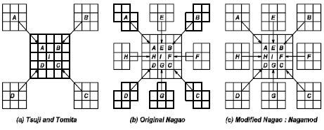
Fig. 1: Neighbourhood Structure
The disadvantage of this technique consists on discarding small regions and this phenomenon is amplified when we iterate this technique many times onto the same image. Nagao et al. have addressed this problem [8] and have proposed a new structure of the neighbourhood (Fig. 1.b) to enhance its performance. The hardware implementation of the nagao filter is not easy to perform because of the irregular mask shapes which complicate enough pixels processing. In addition, computing the variance and the mean requires an important amount of hardware and processing time particularly with the FPGA technologies. In order to simplify its hardware implementation without any video quality regress, Demigny [6] has proposed a modified version in which he considered 9 neighbourhoods of 3x3 pixels with the following centres : A, B, C, D, E, F, G, H and I (Fig. 1.c) without appreciable decreasing of the video quality. In addition, the variance processing is replaced with extent and sum computing. These simplifications allow a new nagao version called Nagamod techniqu..
3. Nagamod Filter
As depicted in the above section, the Nagamod version presents a particular neighbourhood structure which facilitates the hardware implementation of the filter without deteriorating the associated performances. Consider a 5x5 neighbouring pixels, these pixels luminance has some correlation which we would take advantage of. Pixels of intensity related to the current image arrive according to the scanning order of the line. We can consider the image as a mono-dimensional pixels flow. So, two consecutive pixels of the same line are separated with one clock cycle corresponding to the delay z-1 in terms of Z transform. Similarly, two pixels belonging to the same column of two consecutive lines are separated with N clock cycles (delay equal to z-N) where N represents the pixels number per line.
Let’s compare the architecture solutions according to hardware ressources in order to choose the well optimized one to be implemented. The memory resource is one the main criteria to be considered. In all solutions, pixels processing is performed using two blocks: the first one performs the computation of the sum and the distance related to the neighbourhood 5x5, where the second block determines the neighbourhood 3x3 with minimal distance through the three neighbourhoods in order to be matched. In this respect, the Nagamod architecture uses some basic operators to deliver the minimum, the maximum and the extent between three consecutive pixels. In addition, we have to compute the sum and to make the selection between three couples of 3x3 neighbourhoods with specific operators. Consequently, the architecture can be composed by an association of only two basic components named B1 and B2. The B1 component is based on three basic units which give the minimum and the maximum of three pixels and perform the extent and the sum [9]. This block delivers the extent and the sum among 9 of 3x3 neighbourhoods.
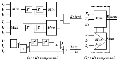
Fig. 2: B1 and B2 components
Given the extent and the sum of the 3x3 pattern as depicted in the Fig. 1.c (A E B) (H I F) and (D G C), we have to determine the minimal extent. The component B2 performs this operation onto the 9 groups of 3x3 neighbourhoods and the minimal extent with its sum (Fig. 2.b).
Nagamod Hardware Solutions
The Nagao filter can be implemented with different organizations according to the performance needs. If we do not have timing constraints, we can implement this algorithm in software manner and obtain the required results. But, if we want to apply this technique to real time application like video smoothing, the software implementation is not suitable and the hardware implementation becomes mandatory. Furthermore, the target architecture can introduce some additional timing constraints. For example FPGA technology has a limited frequency, about 20 MHz, and extended gate delay has strict constraints compared to the ASIC one. Three hardware solutions have been analyzed with equivalent rapidity in order to choose the appropriate one for our hardware environment. The comparison criterion is based on the resources needed in term of memory and controller complexity. We note that the required amount of memory represents the main cost in such architecture. These remarks can be applied for other filter architectures like Sobel and Diriche [10]. In the first solution organization (see figure 3), the architecture is composed of one B1 block working in conjunction with two B2 blocks. The data is buffered both in the input and in the internal part of the architecture. This structure makes the implementation more difficult to perform and particularly the memory controller part.
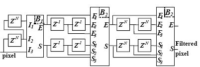
Fig. 3: Solution 1
Fig. 4 shows the overall components of the second hardware solution. This version is compact and requires less amount of memory which can be the external of the computing component.
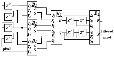
Fig. 4: Solution 2
The third solution, shown in Fig. 5, considers the principle used in the second solution and computes all the operations for two pixels in a parallel way.
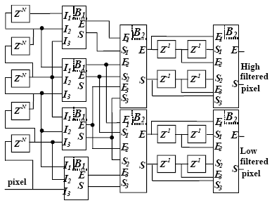
Fig. 5: Solution 3
This solution uses three B1 blocs and four B2 blocs. However, it can be very interesting if we want to compute the gradient behind. In addition, this solution does not require as much memory as that required by the first one. If the delay z-1 is implemented with 8-bit register to code the pixel intensity, a delay z-N is implemented using the FIFO (First In First Out) memory organization to buffer the N pixels intensities of the image line.
4. Nagamod Hardware Implementation
4.1 System Configuration
In order to verify the real-time performance and functionality of the proposed Nagamod filter, a commercially available device, the camera, the grabbing board and the RC1000P-P FPGA based board have been used as depicted in the Fig. 6. The first one, named cyclope board, represents the synchronization one responsible for extracting only the pixel output after grabbing the video with a camera in order to be processed within the FPGA board and restitutes the synchronization before displaying the filtered video sequence. The second borad consists on FPGA prototyping board (RC1000-PP) in which we have to download our architecture bit-stream through the PCI interface of the PC-2.
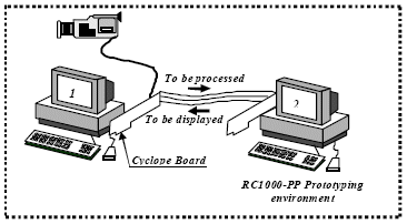
Fig. 6: Scheme of the experimental setup
After being filtered the image pixels intensities are sent to the Cyclope board again in order to be displayed on the screen 1 according to the video standard with a 10MHz frequency clock speed.
4.2 Synchronization Managment
The Cyclope Board presents some specific signals in order to synchronize the image displaying and achieve the real time character without any jerky of the video quality. This board interacts with the camera video grabbing, the prototyping board (RC1000P-P) and the display with the following signals (see figure 7):
- Pixel Clock : For a video flow of 30 images per second, the clock has 10 MHz for a 5122 image size.
- Blank : When it is high, this signal indicates that the received pixels belong to the same line.
- SYNH : This signal periodically gives a negative pulse during the dead time between two consecutive lines belonging to the same image.
- SYNV : In this case, the negative pulse is generated between two consecutive images. This pulse width is equal to the inter-image time.
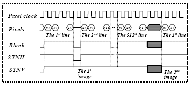
Figure 7: Synchronization video representation
4.3 FPGA Implementation
Our architecture is described with the VHDL language in Register Level Transfer (RTL) according to the second solution presented below in order to be checked onto the FPGA VIRTEX technology. The architecture style relates with a combined data flow with a memory dominated [9,10]. A 720x576 pixel frame must be processed within 40 Ms. Therefore, the processing of one pixel should not exceed 96 Ns (a minimum frequency of 10.3 MHz). The Nagamod architecture consists of three main components such as: the Nagamod filter algorithm, the memory management controller with its dedicated data, and the I/O interface which interacts with the Cyclope board as depicted in the figure 8.
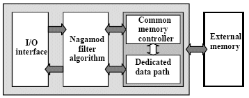
Figure 8: Functional Block Diagram architecture
We remark that the logical organization of the memory requires 4 FIFOs based line storage which are implemented using an external memory device. Remember that implementing FIFO inside the FPGA requires a large consumption number of CLBs [11].
The proposed architecture is synthesized to be checked onto the RC1000P-P, which is a PCI Option Card with an on-board secondary Bus [12]. The RC1000P-P is clocked at 33.33 MHz and can be programmed from the host PC over the PCI bus, or using theXilinx Xchecker download cable. The FPGA has four 32-bit memory ports, one for each one of the four memory banks. It can, therefore, access all four banks simultaneously and independently. This memory implemented the four FIFOs. The access time is about 17 Ns. In order to suit the real time constraints, we have to make a read and write operations related to the two consecutive pixels intensities in the same cycle. We remark that this logical organization architecture requires 4 FIFOs based-line storage which are implemented using an external memory device. Remember that implementing FIFO inside the FPGA requires a large number consumption of CLBs [14].
Our architecture is synthesized to be checked onto the RC1000P-P, which is a PCI Option Card with an onboard secondary Bus [15]. This prototyping board has a XILINX FPGA in BG560 package and Virtex 1000 device. The RC1000P-P is clocked at 33.33 MHz and can be programmed from the host PC over the PCI bus, or using theXilinx Xchecker download cable. In addition, there are four memory banks, as shown in figure. 9 he FPGA has four 32-bit memory ports, one for each memory bank. It can therefore access all four banks simultaneously and independently. Only the SRAM bank0 is used for the Nagamod hardware implementation.
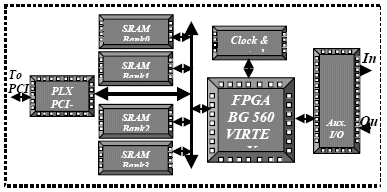
Figure 9 : Block Diagram of the RC1000P-P Board
This memory has implemented the four FIFOs where the access time is about 17 Ns. In order to suit the real time constraints, we have to make a read and write operations related to the two consecutive pixels intensities in the same cycle.
5. Experimental Results
5.1 Qualitative evaluation of the Nagamod Algorithm
The first stage of the experimental part consists on simulating the hardware implementation with ModelSim on the RTL level. We have comapred the smoothing image to the original one captured by a camera. Indeed, we have simulated a 256x256 binary image, containing 256 lines where each line contains 256 pixels with 256-gray scale. The Fig. 11 shows two image configurations before and after the simulation.
By comparing the reconstructed image after smoothing operations with the original one shown in figure. 10, we can appreciate the quality of filtered image. This image has a better contrast and the noise represented by small regions is eliminated. The difference between the two images is well illustrated with the histogram representation.
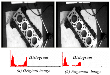
Figure 10: RTL Simulation Results using a 256x256 binary motor block image
In order to prove the efficiency of the nagamod technique and illustrate the smoothing results as a preprocessing phase, we have computed gradient the original image and the Nagamod smoothing one.
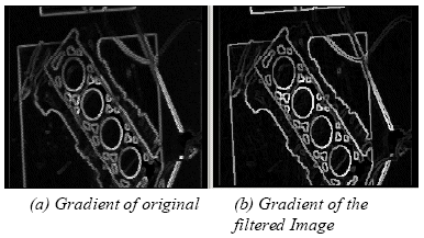
Figure 11: Gradient analysis of filtered image
The Fig. 11 demonstrates the efficiency of the Nagamod algorithm for eliminating noises and improuving the edge detection. We remark that the edge detection is better performed after applying the smoothing technique end an important part of existing noise has been eliminated. Furthermore, the gradient related of filtered image is computed using an image generated with our RTL architecture before synthesis.
Figure 12 presents the RTL simulation related to the memory controller. It shows the manner in reading and buffering data. It also demonstrates the synchronization aspect with enable(Blank) and gnt0(SYNH) signals which are responsible for activating memory operations.
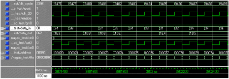
Figure 12: RTL Architecture Simulation Results with ModelSim Tool
5.2 Quantitative Evaluation of the Nagamod
In order to quantify the visual quality of the image after smoothing, we have used the PSNR metric, more appreciated for the video applications than the SNR one. The PSNR is usually defined as:
![]()
Where, MSE is the mean square error given by:
![]()
The PSNR is measured in decibels (dB) where x(m,n) represents the pixels intensity related to the original image and xˆ(m,n) the rebuilt one after smoothing operations. The PSNR remains a good measure for comparing restoration results for the same sequence of image. We have applied our technique onto another image (desk) with a weak contrast. The following table gives the PSNR values related to the two test images.
| Image | PSNR in dB |
| Desk image | 6.89 |
| Motor block image | 16.42 |
Table 1: Architecture requirements
The PSNR measure quantifies the difference between the original image and the smoothed one. It shows the contribution of our technique to enhance the image visual quality. According to the Table 1, the second image with 16.42 dB PSNR may look much better than the other one with 6.89 dB because it has a better contrast and the Nagamod technique suits well with this kind of image.
In the rest of this section, we have to represent the design effort and resources in terms of complexity involved in the generation of the RTL architecture. In the advanced validation process, the RTL description is mapped onto the XILINX bg560 library related to the VIRTEX 1000 family [16] in order to be downloaded onto the RC1000P-P board. In the rest of this section we present the FPGA synthesis results for the main modules of the architecture. The FPGA technology was chosen since it provides some implementation advantages such as: (i) FPGAs provides a high-density for logic arithmetic at relatively short design cycles, (ii) in FPGAs, it is possible to control operations at bit level to build specialized datapaths. The primary results of components synthesis is presented in the Table 2.
| Component | CLB Number | Flop number |
| B1 | 104 | 52 |
| B2 | 32 | 0 |
| Memory controller | 55 | 54 |
| Dedicated data path | 39 | 77 |
| Optimized Nagamod | 435 | 361 |
Table 2: Nagamod Synthesis results
From a temporal view point, the traverse of a data flow through an operator introduces a latency delay between the input and the output. So, the critical path related to the glue logic part of the Nagamod filter has a critical path equal to 25,1 Ns corresponding to the crossing time related to the B1 and B2 components. When we add the memory controller part, we can go beyond the limited delay according to the video frequency 100 ns per period. To overcome this difficulty, we have introduced a two-stage pipeline organisation to divide the critical path onto two cycles.
6. Conclusion
In this paper, we have attempted to show design exploration architecture for real time environment. The detailed architectures for the hardware implementation of the Nagamod technique with all functions and operators have been carried out in a suitable manner. We have discussed the different design solutions. We showed that our proposed solution provides interesting features and suits well with our design and prototyping environment. The architecture has been implemented on a RC1000P-P FPGA of XILINX. The detailed architecture of different block elements of the whole design has been shown. Satisfactory results have been obtained with the FPGA Virtex technology from complexity and speed point of view. Our choice is well justified and gave good results with an optimized memory controller architecture. The proposed architecture reduces the noise in the video sequence and makes the smoothing operation in real-time manner. We reviewed in particular the improvement obtained with the Nagamod algorithm for edge detection and for video visual quality.
7. References
[1] Canny J., 1986. A computational approach to edge detection. IEEE Transactions on Pattern Analysis and Machine Intelligence., 8: 679-698.
[2] Meribout M. and al., 1999. Real-Time Image Segmentation on a Massively Parallel Architecture. Journal of Real-Time Imaging., 5: 279-291.
[3] Kang L. W. and Leou J. J., 2004. An error resilient coding scheme for H.264/AVC video transmission based on data. Journal of Visual Communication and Image Representation., Article in press.
[4] Taubman D. and Marcellin M. W., 2002. JPEG 2000 Image Compression Fundamental Standards and Practice. Kluwer Academic Publishers.
[5] Dantu R. V., Dimopoulos N. J., Li K. F., Patel R. V. and A. J. Al-Khalili A. J., 1994. Parallel algorithms for low-level vision on the homogeneous multiprocessor. Computers & Electrical Engineering., 20: 51-60.
[6] Demigny D., 2001. Méthodes et Architectures pour le TSI en Temps réel. Hermes Editor- Lavoisier. [7] Tomita F. and Tsuji S., 1977. Extraction of Multiple Regions by Smoothing in Selected Neighbourhoods. IEEE Transaction on Systems Man. and Cybernetics., pp: 107-109.
[8] Nagao M. and Matsuyama T., 1979. Edge Preserving Smoothing. Computer Graphics and Image Processing., pp: 394-407.
[9] Demigny D., Devars J., Kessal L. and Quesne J. F., 1993. Implantation temps réel du filtre de lissage d’images de nagao. Revue de Traitement de Signal., 10: 319-329.
[10] Bouguiba R., 2000. Conception d’une architecture matérielle reconfigurable dynamiquement dédiée au traitement d’images en temps réel. PHD thesis at the Cergy-Pontoise University – France.
[11] Vahid F. and Gajski D., 1994. Specification and Design of Embedded Systems. Printice Hall Editor, Englewood Cliffs, NJ.
[12] Fisher G. E., 1994. Rapid System Prototyping in Open System Environment. In Proceedings of International Workshop on Rapid System Prototyping (RSP), Grenoble France.
[13] Djemal R., Mazaré G. and Tourki R., 2000. Rapid Prototyping of an ATM Programmable Associative Operator. Journal of Systems Architectures., 46: 1159- 1173.
[14] Andraka R., 1998. A Survey of CORDIC Algorithm for FPGA Based Computers., pp.191-200.
[15] RC1000P-P. RC1000P-P Hardware Reference manual., INRIA.
[16] APS-X84. VHDL/FPGA Synthsis Tutorial - FPGA Basics.
Related Semiconductor IP
- oFEC Encoder and Decoder
- NPU IP Core for Edge
- NPU IP Core for Mobile
- NPU IP Core for Data Center
- NPU IP Core for Automotive
Related White Papers
- Generic and Automatic Specman based Verification Environment for Image Signal Processing IPs
- Context Based Clock Gating Technique For Low Power Designs of IoT Applications - A DesignWare IP Case Study
- A design of High Efficiency Combo-Type Architecture of MIPI D-PHY and C-PHY
- Extending 8K over a single, cost-effective wire with TICO lightweight compression
Latest White Papers
- Customizing a Large Language Model for VHDL Design of High-Performance Microprocessors
- CFET Beyond 3 nm: SRAM Reliability under Design-Time and Run-Time Variability
- Boosting RISC-V SoC performance for AI and ML applications
- e-GPU: An Open-Source and Configurable RISC-V Graphic Processing Unit for TinyAI Applications
- How to design secure SoCs, Part II: Key Management