A bluetooth radio in 0.18um CMOS
by Paul T.M. van Zeijl, Jan-Wim Eikenbroek, Peter-Paul Vervoort, Suma Setty*, Jurjen Tangenberg, Gary Shipton*, Eric Kooistra, Ids keekstra, Didier Belot**, Klaas Visser, Erwin Bosma, Stephan Blaakmeer.
Ericsson Eurolab Netherlands, Emmen, the Netherlands
* Ericsson Microelectronics, Swindon, UK
** STMicroelectronics, Crolles, France
Abstract :
A bluetooth radio in 0.18 um CMOS technology works on 2.5 - 3.0 V, dissipating 75 mW in RX and 90 mW in TX. RX uses a 2MHz IF with an active poly-phase bandpass filter. The fractional-N PLL uses a VCO running at 5 GHz. TX uses IQ modulation. Special attenation is paid to Si-crosstalk because the radio is combined with baseband circuitry on the same die. The silicon area of the radio is 5.5 mm2.
A BLUETOOTH RADIO IN 0.18 UM CMOS.
The Bluetooth standard is now recognized as a standard for short-range data and voice transfer. Presentations at the ISSCC 2001 [1] and ISSCC 2002 [2], showed a number of solutions in BiCMOS, 0.35 mm CMOS and 0.25 mm CMOS. This paper describes the radio part of a Bluetooth single-chip ASIC in 0.18 mm CMOS, which has a lower current consumption and a smaller Si-area compared to the radios in 0.35 um and 0.25 um CMOS technology.
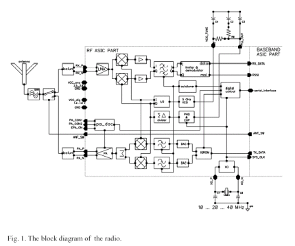
Figure 1 shows the block diagram of the radio. A heterodyne receiver with an active poly-phase filter [3] at an Intermediate Frequency (IF) of 2 MHz is used. The output signal of the bandpass filter is fed to a limiter and then demodulated. The reference voltage for the bandpass filter (and all other filters on silicon) is generated by an autotuner circuit. The autotuner is realized as a PLL coupled to the crystal-oscillator frequency, whereby the VCO in the autotuner is a replica of the gmC stages used in all filters.
The local-oscillator signals for the receiver and transmitter are derived from an oscillator running at 4.8-5.0 GHz. This enables the use of smaller on-chip inductors (and thus smaller silicon-area) with a higher Q, while the Q of the varactors does not significantly influence the oscillator performance. A divide-by-2 circuit generates the required quadrature signals for the RX- and TX-mixers. The PLL incorperates a delta-sigma modulator in the divider-block to enable locking to all Bluetooth channels, for any crystal-oscillator frequency between 10 and 20 MHz. The balanced crystal-oscillator can be trimmed on-frequency by means of two 7 bit capacitor arrays in parallel to the crystal load capacitance. External reference signals can also be injected if available in the application (i.e. 13MHz in GSM).
The transmitter uses IQ-ROM modulation. The low-frequency I- and Q-signals are generated by a ROM and fed to a DAC. After lowpass filtering, mixing and amplification, an on-chip PA delivers +4 dBm to the ASIC pins in a balanced output. An off-chip PA may be used to amplify this signal to +20 dBm. The pa-dac block controls the power level of such a +20 dBm off-chip PA.
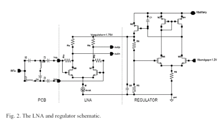
Figure 2 shows the schematic of the LNA. The LNA consists of a differential nMOS pair with resistive loads. The drain-gate feedback resistors, together with the gm of the differential pair and the load resistances determine the input impedance [4]. Inductors are not used to save silicon-area. The noise figure is 3.5 dB at 2.5 GHz with the aid of the balun that transforms the 50 W on the PCB to 150 W on the ASIC. A voltage regulator using thick oxide (7 nm) devices is used to prevent the thin oxide (3.2 nm) devices reaching their breakdown voltage.
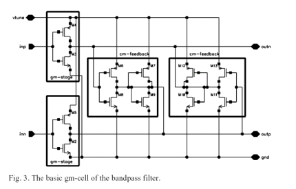
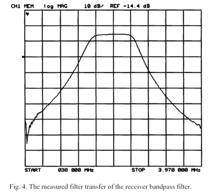
The selectivity filter is a 5th order Butterworth filter with a 1 MHz bandwidth. The active polyphase structure consists of gm and gyrator structures [3]. Figure 3 shows the basic gm-cell. It consists of inverter-stages for the gm, and also for the common-mode feedback [5]. The local power supply voltage of all these inverters determines the filter centre-frequency and is coupled to the reference voltage generated by the autotuner. This inherently decouples the local supply voltage from the battery, thereby increasing power-supply-rejection. MOS capacitances are used as filters capacitances. The sensitivity of this gm-C filter structure to oscillations is analyzed and can be contributed to non-quasi-static effects in the MOS devices. By proper choice of width and length, all compromises (stability, gm-value, capacitance) can be satisfied simultaneously. The filter, together with specially designed driving amplifier, outperforms the Bluetooth distortion/adjacent channel intermodulation specifications. Figure 4 shows the measured transfer curve of the active poly-phase filter. The stop-band rejection is larger then 60 dB.
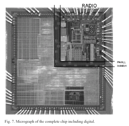
Si-crosstalk is a major issue when radio and baseband are placed on the same ASIC. During the design phase of the project, a substrate model was generated from the floorplan of the ASIC. Simple models were generated for the digital part of the ASIC introducing the concept of "effective inverters" [6], [7]. The combination of these digital effective inverters (modelling up to 1000k gates), the substrate model and the sensitive analog circuitry (like the LNA and the VCO) were then simulated [6], [7]. Several measures are taken for minimising the crosstalk problem: in the layout, a specially designed ptype wall (PWALL, see Figure 7) isolates the radio from the baseband. In the design, all sensitive circuits are balanced and have a high common-mode rejection and a low commonmode to differential-mode-conversion. Separate supplies and power supply regulators are used to increase the power-supply rejection of sensitive circuits like LNA and VCO.
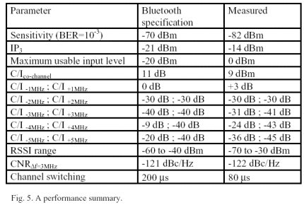
Figure 5 shows a performance summary. The most important Bluetooth specifications are met. First data-transmissions between this Bluetooth ASIC and other Bluetooth radios have already taken place.
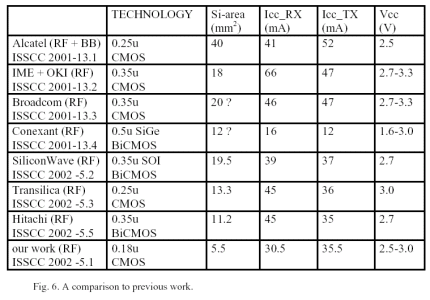
Figure 6 compares papers presented at the ISSCC 2001 [1], at the ISSCC 2002 [2] and this work [2]. This radio is 2-4 times smaller than the IME/OKI, Broadcom, Conexant, Silicon-Wave and Hitachi radios. This radio consumes 30% to 50% less current than CMOS solutions in 0.35 and 0.25 um CMOS.
The STMicroelectronics 0.18 um CMOS process, with 3.2 nm and 7 nm oxide thicknesses, is used. Two extra mask realize a high-Q metal-metal capacitor and a buried-nlayer, giving the possibility of isolating the MOS devices from the substrate. MOS device mismatch includes mismatch in threshold, gm and MOS capacitance such that Monte-Carlo analysis can be used effectively to optimize the silicon area. Figure 7 shows a micrograph of the complete chip. The radio part is the 5.5 mm2 in the right-upper corner.
Acknowledgement:
The authors acknowledge Claude Frank and Elisabeth Cormoreche and their teams from STMicrolelectronics for the supply of the Design Kit and for testing radio performance, respectively, and Sven Mattisson, Christian Bjork, Anders Dunkars, Bojko Marholev, Henrik Geis and Peter Markenlov from Ericsson, Lund, Sweden for discussion.
References:
[1] Session 13 on Bluetooth transceivers, ISSCC Digest of Technical Papers, pp. 194-209, Feb. 2001.[2] Session 5 on Bluetooth transceivers, ISSCC Digest of Technical Papers, pp. 84-95, Feb. 2002.
[3] P. Andreani et all, “A CMOS gmC Polyphase Filter with High Image Band Rejection“, ESSCIRC'2000, Sept. 2000, Stockholm.
[4] E.H. Nordholt, "The Design of High-Performance Negative-Feedback Amplifiers”, Elsevier, 1983.
[5] B. Nauta, “A CMOS Transconductance-C filter technique for Very High Frequencies“, IEEE JSSC, vol. 27, no. 2, Feb. 1992.
[6] P.T.M. van Zeijl, “A Practical Approach in Modelling Silicon-Crosstalk in Systems-On-Silicon", Workshop on Substrate Noise-coupling, IMEC, September 2001, Leuven, Belgium.
[7] S. Donnay, G, Gielen, Editors, “Substrate Noise Coupling in Mixed-0Signals IC's", Chapter 9, Kluwer, to appear at the end of 2002.
Related Semiconductor IP
- 8MHz / 40MHz Pierce Oscillator - X-FAB XT018-0.18µm
- UCIe RX Interface
- Very Low Latency BCH Codec
- 5G-NTN Modem IP for Satellite User Terminals
- 400G UDP/IP Hardware Protocol Stack
Related Articles
- Bluetooth Developer? Why Reinvent the Wireless Radio... Use the CORDIO BT4 Radio IP
- Paving the way for the next generation of audio codec for True Wireless Stereo (TWS) applications - PART 5 : Cutting time to market in a safe and timely manner
- Scalability - A Looming Problem in Safety Analysis
- eFPGAs Bring a 10X Advantage in Power and Cost
Latest Articles
- SNAP-V: A RISC-V SoC with Configurable Neuromorphic Acceleration for Small-Scale Spiking Neural Networks
- An FPGA Implementation of Displacement Vector Search for Intra Pattern Copy in JPEG XS
- A Persistent-State Dataflow Accelerator for Memory-Bound Linear Attention Decode on FPGA
- VMXDOTP: A RISC-V Vector ISA Extension for Efficient Microscaling (MX) Format Acceleration
- PDF: PUF-based DNN Fingerprinting for Knowledge Distillation Traceability