TSMC 40ULP IP
Filter
Compare
38
IP
from
5
vendors
(1
-
10)
-
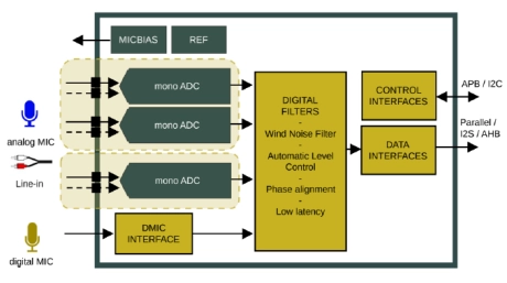
106dB, 24-bit audio three-channels ADC in TSMC 40uLP
- tADC106-SW1-LR.01_TSMC_40_uLP is a mixed (analog and digital) Virtual Component (ViC) in TSMC 40uLP containing a three-channel ADC and additional functions offering an ideal mixed signal front end for low power and high quality audio applications.
-
4608x12 Bits OTP (One-Time Programmable) IP, TSMC 40ULP 0.9V/2.5V Process
- Fully compatible with standard TSMC 40nm ULP 0.9V/2.5V CMOS logic process
- Low voltage: VDD 0.9 V ± 10% for read and program; VDDP: 1.71–3.60 V for read and 2.65 V ± 5% for program
- High speed program: 10-us programming time and support up to dual-bit concurrent programming at one CLK cycle
- High speed read: 10-MHz read clock (100-ns cycle time) per 12-bit word.
-
1Kx8 Bits OTP (One-Time Programmable) IP, TSMC 40ULP 1.1/2.5V Process
- Fully compatible with standard TSMC 40nm ULP 1.1V / 2.5V CMOS process
- Low voltage: VDD 1.1 V ± 10% read and VDDP 2.1 V ± 5% program
- High speed program: 10-us single-bit programming
- High speed read: 9-MHz read clock at 8-bit word.
-
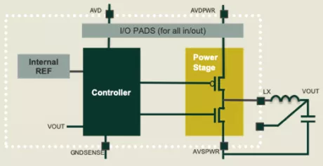
Nano power DC-DC converter in TSMC 40uLP with ultra-low quiescent current and high efficiency at light load
- Low quiescent current suitable for standby modes
- High efficiency at light load extending battery lifetime
- Low ripple level compatible with noise sensitive loads
- Low BoM cost: 1 µH inductor

-
DC/DC buck converter in TSMC 40ULP with low quiescent current and high efficiency at light load
- Low quiescent current suitable for standby modes
- High efficiency at light load extending battery lifetime
- Low ripple level compatible with noise sensitive loads
- Low BoM cost: 1 µH inductor
-
1Kx32 Bits OTP (One-Time Programmable) IP, TSMC 40ULP 1.1/2.5V Process
- Fully compatible with TSMC 40ULP 1.1/2.5V
- Low voltage: 1.1V+/-10% for read and 2.3V+/-0.1V for program
- High speed: 10us program time up to 4 bits at the same time
- Deep sleep mode to cut down power consumption
-
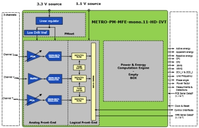
Complete measurement analog front end (AFE) IP for single phase power metering in TSMC 40ULP
- Embedded Computation Engine for utility billing applications
- Low noise Programmable Gain Amplifier (PGA), to reach the best class accuracy with each type of sensors
- Embedded power management for the best resilience to power supply noise
-
PMK Library IPs at TSMC 40ULP Process
- Power-gating cells for domain shutdown
- Isolation cells to prevent unknown states that come from unpowered domains
- Data retention flip-flops
- Always-on cells powered by retention supply rail
- Level shifter cells for multiple voltage domain
-
LPKT Library IPs at TSMC 40ULP Process
- Multi-bit flip-flops to save power and area
- Fine grain cells provide a variety of drive strengths to improve design PPA (Power, Performance, Area)
-
ECO Library IPs at TSMC 40ULP Process
- Ease-of-use, compatible to industrial EDA flow
- Combinational cells (Inverter, Buffer, NAND, NOR, AOI/OAI, XOR/XNR)
- Sequential cells (Scan Flip-flop, and Latch)