SRAM-PUF IP
Filter
Compare
5
IP
from
5
vendors
(1
-
5)
-
GCRAM, the highest-density on-chip embedded memory in standard CMOS
- High-density bitcell offering up-to 2X area reduction over high-density 6T SRAM.
- Full logic compatibility with standard CMOS, no additional process steps or cost.
-
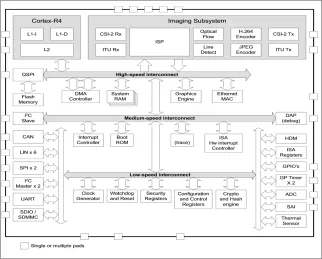
Image Signal Processor (5MP, 2X Sensors) IP
- Self-contained, no external memory needed
- ARM® Cortex-R4 CPU @500 MHz
- Up to 2 Mbytes of SRAM
- Up to 4 Mbytes of stacked Flash or 16 Mbyte external Flash with update via communication interfaces
-
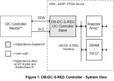
I2C Controller IP – Slave, User Register Interface, No CPU Required
- The DB-I2C-S-REG is an I2C Slave Controller IP Core focused on low VLSI footprint ASIC / ASSP designs not requiring internal configuration & control registers (and thus no local host CPU required). The DB-I2C-S-REG processes the I2C protocol & physical layers, and receives & transmits bytes with respect to the I2C payload to / from User Registers or SRAM/FIFO.
- The DB-I2C-S-REG runs off an external clock input within the ASIC / ASSP, providing a synchronous design while offering I2C spike filtering of SDA and SCL.
-
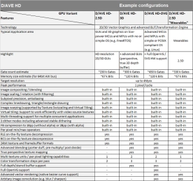
2.5D GPU
- The D/AVE HD 2.5D GPU family is an evolution of the D/AVE 2D family supporting high quality 2D and 3D rendering for displays up to 4K x 4K.
- Targeting modern graphics applications on high resolution displays in the Industrial, Medical, Military, Avionics, Automotive and Consumer markets, the D/AVE HD fixed-function 2.5D GPU core is designed to be fast with powerful functionality.
-
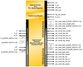
QDRII + SRAM Controller MACO Core
- Interfaces to industry standard QDRII or QDRII+ SRAM
- Supports QDRII SRAM memory devices operating up to 250MHz
- Supports QDRII+ SRAM memory devices operating up to 375MHz (highest speed grade)
- FPGA can be configured for 18-bit or 36-bit read and write memory data buses (on FPGA, 36-bit or 72-bit data buses)